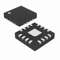
MAX9507ATE+ Maxim Integrated Products, MAX9507ATE+ Datasheet - Page 17

MAX9507ATE+
Manufacturer Part Number
MAX9507ATE+
Description
IC DIRECTDRIVE FILTER AMP 16TQFN
Manufacturer
Maxim Integrated Products
Series
DirectDrive™r
Datasheet
1.MAX9507ATE.pdf
(29 pages)
Specifications of MAX9507ATE+
Applications
Filter
Number Of Circuits
1
-3db Bandwidth
40.7MHz
Slew Rate
35 V/µs
Current - Supply
3.1mA
Current - Output / Channel
82mA
Voltage - Supply, Single/dual (±)
1.7 V ~ 2.63 V
Mounting Type
Surface Mount
Package / Case
16-TQFN Exposed Pad
Supply Current
3.1 mA
Minimum Operating Temperature
- 40 C
Maximum Operating Temperature
+ 125 C
Bandwidth
280 MHz
Maximum Power Dissipation
1250 mW
Mounting Style
SMD/SMT
Supply Voltage (max)
2.625 V
Supply Voltage (min)
1.7 V
For Use With
MAX9507EVKIT+ - KIT EVAL FOR MAX9508MAX9507EVCMAXQU+ - SYSTEM EVAL FOR MAX9507 KIT+MOD
Lead Free Status / RoHS Status
Lead free / RoHS Compliant
Series resistors in line with SDA and SCL are optional.
Series resistors protect the digital inputs of the MAX9507
from high-voltage spikes on the bus lines, and minimize
crosstalk and undershoot of the bus signals.
One data bit is transferred during each SCL cycle. The
data on SDA must remain stable during the high period
of the SCL pulse. Changes in SDA while SCL is high
are control signals (see the START and STOP
Conditions section). SDA and SCL idle high when the
I
SDA and SCL idle high when the bus is not in use. A
master initiates communication by issuing a START con-
dition. A START condition is a high-to-low transition on
SDA with SCL high. A STOP condition is a low-to-high
transition on SDA while SCL is high (Figure 6). A START
condition from the master signals the beginning of a
transmission to the MAX9507. The master terminates
transmission, and frees the bus, by issuing a STOP con-
dition. The bus remains active if a REPEATED START
condition is generated instead of a STOP condition.
The MAX9507 recognizes a STOP condition at any point
during data transmission except if the STOP condition
occurs in the same high pulse as a START condition. For
proper operation, do not send a STOP condition during
the same SCL high pulse as the START condition.
Table 4. Slave Address
Figure 6. START, STOP, and REPEATED START Conditions
2
Load Detection and Dual SPST Analog Switches
C bus is not busy.
DEV_ADDR
SCL
SDA
GND
SCL
SDA
V
DD
S
1.8V DirectDrive Video Filter Amplifier with
B7
1
1
1
1
______________________________________________________________________________________
START and STOP Conditions
B6
0
0
0
0
Sr
Early STOP Conditions
B5
0
0
0
0
B4
1
1
1
1
Bit Transfer
B3
1
1
1
1
P
B2
0
0
1
1
B1
0
1
0
1
The slave address is defined as the 7 most significant
bits (MSBs) followed by the read/write (R/W) bit. Set the
R/W bit to 1 to configure the MAX9507 to read mode.
Set the R/W bit to 0 to configure the MAX9507 to write
mode. The slave address is always the first byte of
information sent to the MAX9507 after a START or a
REPEATED START condition. The MAX9507 slave
address is configurable with DEV_ADDR. Table 4
shows the possible slave addresses for the MAX9507.
The acknowledge bit (ACK) is a clocked 9th bit that the
MAX9507 uses to handshake receipt of each byte of data
when in write mode (see Figure 7). The MAX9507 pulls
down SDA during the entire master-generated ninth clock
pulse if the previous byte is successfully received.
Monitoring ACK allows for detection of unsuccessful data
transfers. An unsuccessful data transfer occurs if a
receiving device is busy or if a system fault has occurred.
In the event of an unsuccessful data transfer, the bus
master may retry communication. The master pulls down
SDA during the ninth clock cycle to acknowledge receipt
of data when the MAX9507 is in read mode. An acknowl-
edge is sent by the master after each read byte to allow
data transfer to continue. A not acknowledge is sent
when the master reads the final byte of data from the
MAX9507, followed by a STOP condition.
Figure 7. Acknowledge
SDA
SCL
CONDITION
START
R/W
R/W
R/W
R/W
B0
WRITE ADDRESS
1
(hex)
0x9C
0x9A
0x9E
0x98
2
NOT ACKNOWLEDGE
ACKNOWLEDGE
ACKNOWLEDGMENT
8
READ ADDRESS
CLOCK PULSE FOR
Slave Address
Acknowledge
(hex)
0x9D
0x99
0x9B
0x9F
9
17


