AD813ANZ Analog Devices Inc, AD813ANZ Datasheet - Page 6
AD813ANZ
Manufacturer Part Number
AD813ANZ
Description
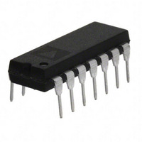
IC OPAMP TRIPLE VIDEO LP 14DIP
Manufacturer
Analog Devices Inc
Datasheet
1.AD813ARZ-14.pdf
(19 pages)
Specifications of AD813ANZ
Slew Rate
250 V/µs
Applications
Current Feedback
Number Of Circuits
3
-3db Bandwidth
100MHz
Current - Supply
4.5mA
Current - Output / Channel
50mA
Voltage - Supply, Single/dual (±)
2.4 V ~ 36 V, ±1.2 V ~ 18 V
Mounting Type
Through Hole
Package / Case
14-DIP (0.300", 7.62mm)
Gain Bandwidth
125MHz
Supply Voltage Range
2.4V To 36V
No. Of Amplifiers
3
Output Current
50mA
Amplifier Output
Single Ended
Operating Temperature Range
-40°C To +85°C
Lead Free Status / RoHS Status
Lead free / RoHS Compliant
Available stocks
Company
Part Number
Manufacturer
Quantity
Price
Company:

Part Number:
AD813ANZ
Manufacturer:
MAXIM
Quantity:
17 513


AD813
Maximum Power Dissipation
The maximum power that can be safely dissipated by the
AD813 is limited by the associated rise in junction temperature.
The maximum safe junction temperature for the plastic encap-
sulated parts is determined by the glass transition temperature
of the plastic, about 150 C. Exceeding this limit temporarily
may cause a shift in parametric performance due to a change in
the stresses exerted on the die by the package. Exceeding a
junction temperature of 175 C for an extended period can result
in device failure.
While the AD813 is internally short circuit protected, this may
not be enough to guarantee that the maximum junction tem-
perature (150 C) is not exceeded under all conditions. To
ensure proper operation, it is important to observe the derating
curves.
It must also be noted that in (noninverting) gain configurations
(with low values of gain resistor), a high level of input overdrive
can result in a large input error current, which may result in a
significant power dissipation in the input stage. This power
must be included when computing the junction temperature rise
due to total internal power.
CAUTION
ESD (electrostatic discharge) sensitive device. Electrostatic charges as high as 4000 V readily
accumulate on the human body and test equipment and can discharge without detection.
Although the AD813 features proprietary ESD protection circuitry, permanent damage may
occur on devices subjected to high energy electrostatic discharges. Therefore, proper ESD
precautions are recommended to avoid performance degradation or loss of functionality.
DISABLE2 2
DISABLE1 1
OUT2 14
–IN2 13
+IN2
12
DISABLE3
3
0.124
(3.15)
V
Dimensions shown in inches and (mm).
4
S
+
METALIZATION PHOTO
V
11
S
–
–6–
V
11
Figure 3. Maximum Power Dissipation vs. Ambient
Temperature
S
–
+IN1
5
V
11
2.5
2.0
1.5
1.0
0.5
S
–50
–
–40
–30
14-LEAD SOIC
–20
+IN3
–10
AMBIENT TEMPERATURE – C
10
–IN1
0
6
10
9 –IN3
8 OUT3
7 OUT1
20 30 40
WARNING!
14-LEAD DIP PACKAGE
(1.45)
0.057
50
ESD SENSITIVE DEVICE
60 70
T
J
= +150 C
80
90
REV. B
Related parts for AD813ANZ
Image
Part Number
Description
Manufacturer
Datasheet
Request
R

Part Number:
Description:
±1.7g Dual-Axis IMEMS Accelerometer Evaluation Board
Manufacturer:
Analog Devices Inc
Datasheet:

Part Number:
Description:
Inertial Sensor Evaluation System
Manufacturer:
Analog Devices Inc
Datasheet:
Part Number:
Description:
Manufacturer:
Analog Devices Inc
Datasheet:
Part Number:
Description:
Manufacturer:
Analog Devices Inc
Datasheet:
Part Number:
Description:
Manufacturer:
Analog Devices Inc
Datasheet:
Part Number:
Description:
Manufacturer:
Analog Devices Inc
Datasheet:
Part Number:
Description:
Manufacturer:
Analog Devices Inc
Datasheet:
Part Number:
Description:
Manufacturer:
Analog Devices Inc
Datasheet:
Part Number:
Description:
Manufacturer:
Analog Devices Inc
Datasheet:
Part Number:
Description:
Manufacturer:
Analog Devices Inc
Datasheet:
Part Number:
Description:
Manufacturer:
Analog Devices Inc
Datasheet:
Part Number:
Description:
Manufacturer:
Analog Devices Inc
Datasheet:
Part Number:
Description:
Manufacturer:
Analog Devices Inc
Datasheet: