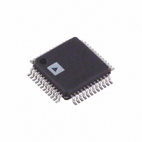
ADAU1701JSTZ Analog Devices Inc, ADAU1701JSTZ Datasheet - Page 39

ADAU1701JSTZ
Manufacturer Part Number
ADAU1701JSTZ
Description
IC AUDIO PROC 2ADC/4DAC 48-LQFP
Manufacturer
Analog Devices Inc
Series
SigmaDSP®r
Type
Audio Processorr
Specifications of ADAU1701JSTZ
Design Resources
Analog Audio Input, Class-D Output with ADAU1701, SSM2306, and ADP3336 (CN0162)
Applications
Automotive, Monitors, MP3
Mounting Type
Surface Mount
Package / Case
48-LQFP
Audio Control Type
Digital
Control Interface
I2C, Serial
Supply Voltage Range
1.8V, 3.3V
Operating Temperature Range
0°C To +70°C
Audio Ic Case Style
LQFP
No. Of Pins
48
Svhc
No SVHC
Control / Process Application
MP3 Player Speaker Docks, Automotive Head Units, Studio Monitors
Rohs Compliant
Yes
Lead Free Status / RoHS Status
Lead free / RoHS Compliant
For Use With
EVAL-ADAU1701MINIZ - BOARD EVAL SIGMADSP AUD ADAU1701EVAL-ADAU1701EBZ - BOARD EVAL FOR ADAU1701
Lead Free Status / RoHS Status
Lead free / RoHS Compliant, Lead free / RoHS Compliant
Available stocks
Company
Part Number
Manufacturer
Quantity
Price
Company:
Part Number:
ADAU1701JSTZ
Manufacturer:
Analog Devices Inc
Quantity:
1 923
Company:
Part Number:
ADAU1701JSTZ
Manufacturer:
ADI
Quantity:
221
Company:
Part Number:
ADAU1701JSTZ
Manufacturer:
Analog Devices Inc
Quantity:
10 000
Part Number:
ADAU1701JSTZ
Manufacturer:
ADI/亚德诺
Quantity:
20 000
Company:
Part Number:
ADAU1701JSTZ-RL
Manufacturer:
ON
Quantity:
35 000
Company:
Part Number:
ADAU1701JSTZ-RL
Manufacturer:
Analog Devices Inc
Quantity:
10 000
Part Number:
ADAU1701JSTZ-RL
Manufacturer:
ADI/亚德诺
Quantity:
20 000
2079 (0x081F)—SERIAL INPUT CONTROL REGISTER
Table 50.
D7
0
Table 51.
Bit Name
ILP
IBP
M [2:0]
INPUT_LRCLK Polarity
INPUT_BCLK Polarity
Serial Input Mode
D6
0
Description
When this bit is set to 0, the left-channel data on the SDATA_INx pins is clocked when INPUT_LRCLK is low and
the right-channel data is clocked when INPUT_LRCLK is high. When this bit is set to 1, the clocking of these
channels is reversed. In TDM mode when this bit is set to 0, data is clocked in, starting with the next appropriate
BCLK edge (set in Bit 3 of this register) after a falling edge on the INPUT_LRCLK pin. When this bit is set to 1 and
the device is running in TDM mode, the input data is valid on the BCLK edge after a rising edge on the word
clock (INPUT_LRCLK). INPUT_LRCLK can also operate with a pulse input, rather than a clock. In this case, the first
edge of the pulse is used by the ADAU1701 to start the data frame. When this polarity bit is set to 0, a low pulse
should be used; when the bit it set to 1, a high pulse should be used.
This bit controls on which edge of the bit clock the input data changes and on which edge it is clocked. Data
changes on the falling edge of INPUT_BCLK when this bit is set to 0 and on the rising edge when this bit is set at 1.
These two bits control the data format that the input port expects to receive. Bit 3 and Bit 4 of this control
register override the settings of Bits 2:0; therefore, all four bits must be changed together for proper operation
in some modes. The clock diagrams for these modes are shown in Figure 31, Figure 32, and Figure 33. Note that
for left-justified and right-justified modes the LRCLK polarity is high and then low, which is opposite from the
default setting of ILP.
When these bits are set to accept a TDM input, the ADAU1701 data starts after the edge defined by ILP. The
ADAU1701 TDM data stream should be input on Pin SDATA_IN0. Figure 34 shows a TDM stream with a high-to-
low triggered LRCLK and data changing on the falling edge of the BCLK. The ADAU1701 expects the MSB of
each data slot to be delayed by one BCLK from the beginning of the slot, as it would in stereo I
mode, Channel 0 to Channel 3 are in the first half of the frame, and Channel 4 to Channel 7 are in the second
half. Figure 35 shows an example of a TDM stream running with a pulse word clock, which is used to interface to
ADI codecs in auxiliary mode. To work in this mode with either the input or output serial ports, set the
ADAU1701 to begin the frame on the rising edge of LRCLK, to change data on the falling edge of BCLK, and to
delay the MSB position from the start of the word clock by one BCLK.
M [2:0]
000
001
010
011
100
101
110
111
D5
0
Setting
I
Left justified
TDM
Right justified, 24 bits
Right justified, 20 bits
Right justified, 18 bits
Right justified, 16 bits
Reserved
2
S
D4
ILP
Rev. 0 | Page 39 of 52
D3
IBP
D2
M2
D1
M1
M0
D0
2
S format. In TDM
ADAU1701
Default
0x00


