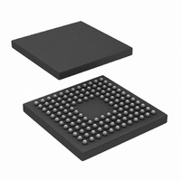
CLC5903SM/NOPB National Semiconductor, CLC5903SM/NOPB Datasheet - Page 17

CLC5903SM/NOPB
Manufacturer Part Number
CLC5903SM/NOPB
Description
IC DGTL TUNER/AGC DUAL 128-FBGA
Manufacturer
National Semiconductor
Type
Tunerr
Datasheet
1.CLC5903SMNOPB.pdf
(29 pages)
Specifications of CLC5903SM/NOPB
Applications
Base Stations
Mounting Type
Surface Mount
Package / Case
128-FBGA
Lead Free Status / RoHS Status
Lead free / RoHS Compliant
Other names
*CLC5903SM
*CLC5903SM/NOPB
CLC5903SM
*CLC5903SM/NOPB
CLC5903SM
Available stocks
Company
Part Number
Manufacturer
Quantity
Price
Company:
Part Number:
CLC5903SM/NOPB
Manufacturer:
Texas Instruments
Quantity:
10 000
decreases relative to the output sample rate, the CIC droop
compensation performed by F1 may no longer be required.
Overall Channel Gain
The overall gain of the chip is a function of the amount of
decimation (N), the settings of the “SHIFT UP” circuit
(SCALE), the GAIN setting, the sum of the F1 coefficients,
and the sum of the F2 coefficients. The overall gain is shown
below in Equation 2.
Where:
and:
It is assumed that the DDC output words are treated as frac-
tional 2’s complement words. The numerators of
F1 and F2, respectively. For the STD and GSM sets,
and
term in (2) is cancelled by the DVGA operation so that the
entire gain of the DRCS is independent of the DVGA setting
when EXP_INH=0. The
Output Modes
G
F2
G
Figure 28. CIC, F1, & F2 GSM Passband Flatness
G
−0.5
−1.5
0.5
DDC
equal the sums of the impulse response coefficients of
−1
−2
F2
1
0
0
are nearly equal to unity. Observe that the
=
Combined Frequency Response of CIC/F1/F2 Using GSM Set
1
-- - DEC
2
2
2
G
GAIN
20
F1
SCALE 44
G
G
G
+
F1
F2
F2
1
1
-- -
2
(Continued)
–
=
=
4
40
Frequency (KHz)
appearing in (2) is the result of the
i
---------------------- -
i
---------------------- -
–
∑
∑
21
63
=
=
AGAIN
1
2
1
2
h
h
16
16
1
2
i
i
60
1 EXP_INH
–
80
G
AGAIN
F1
100
G
and
(2)
(3)
(4)
F1
17
6dB conversion loss in the mixer. For full-scale square wave
inputs the
Data Latency and Group Delay
The CLC5903 latency calculation assumes that the FIR filter
latency will be equal to the time required for data to propa-
gate through one half of the taps. The CIC filter provides 4N
equivalent taps where N is the CIC decimation ratio. F1 and
F2 provide 21 and 63 taps respectively. When these filters
are reflected back to the input rate, the effective taps are
increased by decimation. This results in a total of 298N taps
when the F2 decimation is 2 and 550N taps when the F2
decimation is 4.
The latency is then 149N CK periods when the F2 decima-
tion is 2 and 275N CK periods when the F2 decimation is 4.
The CLC5903 filters are linear phase filters so the group
delay remains constant.
Output Modes
After processing by the DDC, the data is then formatted for
output.
All output data is two’s complement. The serial outputs
power up in a tri-state condition and must be enabled
when the chip is configured. Parallel outputs are
enabled by the POUT_EN pin.
Output formats include truncation to 8 or 32 bits, rounding to
16 or 24 bits, and a 12-bit floating point format (4-bit expo-
nent, 8-bit mantissa, 138dB numeric range). This function is
performed in the OUTPUT CIRCUIT shown in Figure 29.
The channel outputs are accessible through serial output
pins and a 16-bit parallel output port. The RDY pin is pro-
vided to notify the user that a new output sample period
(OSP) has begun. OSP refers to the interval between output
samples at the decimated output rate. For example, if the
input rate (and clock rate) is 52 MHz and the overall decima-
tion factor is 192 (N=48, F2 decimation=2) the OSP will be
3.69 microseconds which corresponds to an output sample
CK
1
-- -
2
RDY_POL, SCK_POL, SFS_POL
DIVIDE
Figure 29. CLC5903 output circuit
RATE
should be set to 1 to prevent signal distortion.
BY
MUX
16
3
RDY
SCK
SFS
AOUT
BOUT
SCK_IN
POUT[15..0]
POUT_SEL[2..0]
POUT_EN
www.national.com


