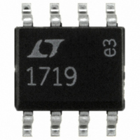
LT1719CS8#PBF Linear Technology, LT1719CS8#PBF Datasheet

LT1719CS8#PBF
Specifications of LT1719CS8#PBF
Available stocks
Related parts for LT1719CS8#PBF
LT1719CS8#PBF Summary of contents
Page 1
... The SO-8 package has separate supplies which allow flexible operation, accomodating separate analog input ranges and output logic levels. For a dual/quad comparator with similar performance, see the LT1720/LT1721. , LTC and LT are registered trademarks of Linear Technology Corporation. UltraFast is a trademark of Linear Technology Corporation ...
Page 2
LT1719 ABSOLUTE MAXIMUM (Note 1) Supply Voltage + V to GND (LT1719S8) ...................................... (LT1719S8) ....................................... 12V (LT1719S8) ...................................... 12V GND (LT1719S8) ...................... ...
Page 3
ELECTRICAL CHARACTERISTICS range, otherwise specifications are and V = –5V, for the LT1719S6 SYMBOL PARAMETER V Output Low Voltage OL t Propagation Delay PD20 t Propagation Delay PD5 ...
Page 4
LT1719 ELECTRICAL CHARACTERISTICS Note 8: Because of internal hysteresis, there is no small-signal region in which to measure gain. Proper operation of internal circuity is ensured by measuring V and V with only 10mV of overdrive Note 9: ...
Page 5
W U TYPICAL PERFORMANCE CHARACTERISTICS Propagation Delay vs Load Capacitance RISING EDGE 100mV STEP (t ) PDLH OVERDRIVE = 20mV + – ...
Page 6
LT1719 W U TYPICAL PERFORMANCE CHARACTERISTICS Shutdown Currents vs Temperature SHUTDOWN = +V – 0. SHUTDOWN PIN OPEN 0.1 –50 – TEMPERATURE ( PIN FUNCTIONS LT1719S8 V (Pin 1): Positive ...
Page 7
TEST CIRCUITS PULSE 0V IN –3V 50 BANDWIDTH-LIMITED TRIANGLE WAVE ~ 1kHz 0.1 F 50k + DUT 50 LT1719 50 – 200k V CM 1/2 LT1638 100k 100k + – + 100k – 100k 1/2 ...
Page 8
LT1719 U U APPLICATIONS INFORMATION Power Supply Configurations (SO-8 Package) The LT1719S8 has separate supply pins for the input and output stages that allow flexible operation, accommodat- ing separate voltage ranges for the analog input and the output logic. Of ...
Page 9
U U APPLICATIONS INFORMATION equal to the supply voltage, limited only by the absolute maximum currents noted. External input protection cir- cuitry is only needed if currents would otherwise exceed these absolute maximums. The internal catch diodes can conduct current ...
Page 10
LT1719 U U APPLICATIONS INFORMATION shutdown is active high, this resistor adds little power drain during shutdown. A logic high disables the compara- tor. The LT1719S8 logic interface is based on the output power rails and GND. S ...
Page 11
U U APPLICATIONS INFORMATION Additional hysteresis may be added externally. The rail-to- rail outputs of the LT1719 make this more predictable than with TTL output comparators due to the LT1719’s small variability of V (output high voltage add ...
Page 12
LT1719 U U APPLICATIONS INFORMATION Interfacing the LT1719 to ECL The LT1719 comparators can be used in high speed applications where Emitter-Coupled Logic (ECL) is de- ployed. To interface the output of the LT1719 to ECL logic inputs, standard TTL/CMOS ...
Page 13
U U APPLICATIONS INFORMATION Figure 6a shows the standard TTL to Positive ECL (PECL) resistive level translator. This translator cannot be used for the LT1719, or with CMOS logic, because it depends on the 820 resistor to limit the output ...
Page 14
LT1719 U U APPLICATIONS INFORMATION Circuit Description The block diagram of the LT1719 is shown in Figure 7. The circuit topology consists of a differential input stage, a gain stage with hysteresis and a complementary com- mon-emitter output stage. All ...
Page 15
U U APPLICATIONS INFORMATION Speed Limits The LT1719 comparator is intended for high speed appli- cations, where it is important to understand a few limita- tions. These limitations can roughly be divided into three categories: input speed limits, output speed ...
Page 16
LT1719 U U APPLICATIONS INFORMATION V Test Circuit TRIP The input trip points test circuit uses a 1kHz triangle wave to repeatedly trip the comparator being tested. The LT1719 output is used to trigger switched capacitor sampling of the triangle ...
Page 17
PLIFIED SCHE ATIC LT1719 17 ...
Page 18
LT1719 PACKAGE DESCRIPTION 0.010 – 0.020 (0.254 – 0.508) 0.008 – 0.010 (0.203 – 0.254) 0.016 – 0.050 (0.406 – 1.270) * DIMENSION DOES NOT INCLUDE MOLD FLASH. MOLD FLASH SHALL NOT EXCEED 0.006" (0.152mm) PER SIDE ** DIMENSION DOES ...
Page 19
... SC-74A (EIAJ) FOR ORIGINAL JEDEC MO-193 FOR THIN Information furnished by Linear Technology Corporation is believed to be accurate and reliable. However, no responsibility is assumed for its use. Linear Technology Corporation makes no represen- tation that the interconnection of its circuits as described herein will not infringe on existing patent rights. U Dimensions in inches (millimeters) unless otherwise noted ...
Page 20
... A Single Supply Comparator Rail-to-Rail Inputs and Outputs Dual/Quad Comparator Similar to the LT1719 sine wave at P-P at 10MHz, the LT1719 delay starts to de – 10MHz 632mV 2V 6.32V P-P P-P P INPUT AMPLITUDE (dBm) 1719 F08b 1719f LT/TP 1100 4K • PRINTED IN USA LINEAR TECHNOLOGY CORPORATION 2000 ...


