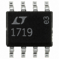
LT1719CS8#PBF Linear Technology, LT1719CS8#PBF Datasheet - Page 14

LT1719CS8#PBF
Manufacturer Part Number
LT1719CS8#PBF
Description
IC COMP R-R I/O SGL 3/5V 8-SOIC
Manufacturer
Linear Technology
Series
UltraFast™r
Type
General Purposer
Specifications of LT1719CS8#PBF
Number Of Elements
1
Output Type
CMOS, Rail-to-Rail, TTL
Voltage - Supply
2.7 V ~ 10.5 V
Mounting Type
Surface Mount
Package / Case
8-SOIC (0.154", 3.90mm Width)
Comparator Type
General Purpose
No. Of Comparators
1
Response Time
4.5ns
Ic Output Type
CMOS, TTL
Output Compatibility
CMOS, TTL
Supply Current
4.2mA
Supply Voltage Range
2.7V To 10.5V
Rohs Compliant
Yes
Lead Free Status / RoHS Status
Lead free / RoHS Compliant
Available stocks
Company
Part Number
Manufacturer
Quantity
Price
APPLICATIONS
LT1719
Circuit Description
The block diagram of the LT1719 is shown in Figure 7. The
circuit topology consists of a differential input stage, a
gain stage with hysteresis and a complementary com-
mon-emitter output stage. All of the internal signal paths
utilize low voltage swings for high speed at low power.
The input stage topology maximizes the input dynamic
range available without requiring the power, complexity
and die area of two complete input stages such as are
found in rail-to-rail input comparators. With a single 2.7V
supply, the LT1719 still has a respectable 1.6V of input
common mode range. The differential input voltage range
is rail-to-rail, without the large input currents found in
competing devices. The input stage also features phase
reversal protection to prevent false outputs when the
inputs are driven below the –100mV common mode
voltage limit.
14
+IN
–IN
–
+
V
V
A
CC
EE
V1
OR V
U
OR V
+
–
SHUTDOWN
INFORMATION
U
+
+
W
NONLINEAR STAGE
+
–
BIAS CONTOL
A
V2
Figure 7. LT1719 Block Diagram
U
The internal hysteresis is implemented by positive, nonlin-
ear feedback around a second gain stage. Until this point,
the signal path has been entirely differential. The signal
path is then split into two drive signals for the upper and
lower output transistors. The output transistors are con-
nected common emitter for rail-to-rail output operation.
The Schottky clamps limit the output voltages at about
300mV from the rail, not quite the 50mV or 15mV of Linear
Technology’s rail-to-rail amplifiers and other products.
But the output of a comparator is digital, and this output
stage can drive TTL or CMOS directly. It can also drive ECL,
as described earlier, or analog loads as demonstrated in
the applications to follow.
The bias conditions and signal swings in the output stage
are designed to turn their respective output transistors off
faster than on. This helps minimize the surge of current
from + V
minimize the frequency-dependent increase in power con-
sumption. The frequency dependence of the supply cur-
rent is shown in the Typical Performance Characteristics.
–
–
+
+
S
/ V
+
to ground that occurs at transitions, to
GND OR V
+V
OUT
S
OR V
1719 F07
+
–


