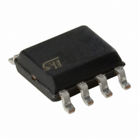
TSM109AIDT STMicroelectronics, TSM109AIDT Datasheet - Page 3

TSM109AIDT
Manufacturer Part Number
TSM109AIDT
Description
IC CTRLR DUAL COMP/VREF 8SOIC
Manufacturer
STMicroelectronics
Type
with Voltage Referencer
Datasheet
1.TSM109AIDT.pdf
(7 pages)
Specifications of TSM109AIDT
Number Of Elements
2
Voltage - Supply
2 V ~ 36 V, ±1 V ~ 18 V
Mounting Type
Surface Mount
Package / Case
8-SOIC (0.154", 3.90mm Width)
Output Current
1 mA
Input Voltage
2 V to 36 V
Operating Temperature Range
- 40 C to + 105 C
Mounting Style
SMD/SMT
Number Of Outputs
2
Number Of Elements
2
Technology
Bipolar
Input Offset Voltage
5mV
Input Bias Current (typ)
25nA
Response Time
1.3us
Single Supply Voltage (typ)
3/5/9/12/15/18/24/28V
Dual Supply Voltage (typ)
±3/±5/±9/±12/±15V
Supply Current (max)
1@5VmA
Power Supply Requirement
Single/Dual
Voltage Gain In Db
106.02dB
Single Supply Voltage (min)
2V
Single Supply Voltage (max)
36V
Dual Supply Voltage (min)
±1V
Dual Supply Voltage (max)
±18V
Operating Temp Range
-40C to 105C
Operating Temperature Classification
Industrial
Mounting
Surface Mount
Pin Count
8
Package Type
SO
Lead Free Status / RoHS Status
Request inventory verification / Request inventory verification
Other names
497-4082-2
Available stocks
Company
Part Number
Manufacturer
Quantity
Price
Company:
Part Number:
TSM109AIDT
Manufacturer:
STMicroelectronics
Quantity:
1 865
Electrical Characteristics
2
COMPARATOR (independent comparator)
V
1)
2)
3)
4)
5)
Symbo
CC
V
V
I
A
I
V
V
sink
t
t
I
I
OH
rel
icm
ELECTRICAL CHARACTERISTICS
+
l
io
ib
OL
re
The response time specified is for a 100mV input step with 5mV overdrive. For larger overdrive signals, 300ns can be obtained
vd
io
id
At output switch point, V
The direction of the input current is out of the IC due to the PNP input stage. This current is essentially constant, independent of the
state of the output, so no loading charge exists on the reference of input lines.
The input common-mode voltage of either input signal voltage should not be allowed to go negative by more than 0.3V. The upper end
of the common-mode voltage range is V
Positive voltage excursions of one input may exceed the power supply level. As long as the other input voltage remains within the
common-mode range, the comparator will provide an appropriate output state. The low input voltage state must not be less than -0.3V
(or 0.3V below the negative power supply, if used).
= +5V, V
Input Offset Voltage - note
T
T
Input Offset Current
T
T
Input Bias Current (I
T
T
Large Signal Voltage Gain
V
Input Common Mode Voltage Range - note
V
T
T
Differential Input Voltage -note
Low Level Output Voltage
V
T
T
High Level Output Current (V
V
T
T
Output Sink Currrent
V
Response Time - note
R
Large Signal Response Time
R
V
amb
amb
amb
amb
amb
amb
min
min
min
min
min
min
CC
CC
id
CC
id
L
L
(ref)
= 5.1k
= 5.1k
= 1V, V
= -1V, I
= 15V, R
= 30V
= V
= +25°C
= +25°C
= +25°C
= +25°C
= +25°C
= +25°C
= +1.4v
CC
T
T
T
T
T
T
o
amb
amb
amb
amb
amb
amb
-
= 30V
= GND, T
sink
o
connected to V
connected to V
= 1.5V
L
= 4mA
T
T
T
T
T
T
= 15k
o
max
max
max
max
max
max
1.4V, R
+
or I
amb
5
V
o
s
-
) - note
CC
CC
= +25°C (unless otherwise specified)
= 0 with V
= 1V to 11V
1
+
+
id
CC
, e
Parameter
4
= 1V)
+
l
-1.5V.
= TTL,
2
CC
+
from 5V to 30V, and over the full common-mode range (0V to V
3
Min. Typ.
50
10
0
0
TSM109
200
250
300
1.3
25
30
20
1
3
V
V
CC
Max.
V
CC
CC
100
250
400
400
700
150
25
CC
TSM109/A
+
5
9
1
+
+
-1.5
-1.5V).
+
-2
V/mV
Unit
mV
mV
mA
nA
nA
nA
ns
V
A
s
3/7


