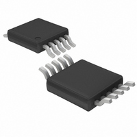
LT1715CMS#PBF Linear Technology, LT1715CMS#PBF Datasheet - Page 10

LT1715CMS#PBF
Manufacturer Part Number
LT1715CMS#PBF
Description
IC COMPARATOR 150MHZ DUAL 10MSOP
Manufacturer
Linear Technology
Series
UltraFast™r
Type
General Purposer
Specifications of LT1715CMS#PBF
Number Of Elements
2
Output Type
CMOS, Rail-to-Rail, TTL
Voltage - Supply
2.7 V ~ 12 V
Mounting Type
Surface Mount
Package / Case
10-TFSOP, 10-MSOP (0.118", 3.00mm Width)
Comparator Type
High Speed
No. Of Comparators
2
Response Time
4ns
Ic Output Type
CMOS, TTL
Supply Current
1mA
Supply Voltage Range
2.7V To 12V
Amplifier Case Style
MSOP
No. Of Pins
10
Rohs Compliant
Yes
Output Compatibility
CMOS, TTL
Lead Free Status / RoHS Status
Lead free / RoHS Compliant
Available stocks
Company
Part Number
Manufacturer
Quantity
Price
APPLICATIO S I FOR ATIO
LT1715
At frequencies well beyond 100MHz, the toggling of one
channel may be impaired by toggling on the other. This is
a rather complex interaction of supply bypassing and bond
inductance, and it cannot be entirely prevented. However,
good bypassing and board layout techniques will effec-
tively minimize it.
Power Supply Sequencing
The LT1715 is designed to tolerate any power supply
sequencing at system turn-on and power down. In any of
the previously shown power supply configurations, the
various supplies can activate in any order without exces-
sive current drain by the LT1715.
As always, the Absolute Maximum Ratings must not be
exceeded, either on the power supply terminals or the
input terminals. Power supply sequencing problems can
occur when input signals are powered from supplies that
are independent of the LT1715’s supplies. No problems
should occur if the input signals are powered from the
same V
Unused Comparators
If a comparator is unused, its output should be left floating
to minimize load current. The unused inputs can be tied off
to the rails and power consumption can be further mini-
mized if the inputs are connected to the power rails to
induce an output low. Connecting the inverting input to
V
easiest method.
Hysteresis
The LT1715 includes internal hysteresis, which makes it
easier to use than many other similar speed comparators.
The input-output transfer characteristic is illustrated in
Figure 5 showing the definitions of V
upon the two measurable trip points. The hysteresis band
makes the LT1715 well behaved, even with slowly moving
inputs.
The exact amount of hysteresis will vary from part to part
as indicated in the specifications table. The hysteresis
level will also vary slightly with changes in supply voltage
and common mode voltage. A key advantage of the
10
CC
and the noninverting input to V
CC
and V
EE
supplies as the LT1715.
U
U
W
OS
EE
and V
will likely be the
HYST
U
based
LT1715 is the significant reduction in these effects, which
is important whenever an LT1715 is used to detect a
threshold crossing in one direction only. In such a case,
the relevant trip point will be all that matters, and a stable
offset voltage with an unpredictable level of hysteresis, as
seen in competing comparators, is useless. The LT1715 is
many times better than prior generation comparators in
these regards. In fact, the CMRR and PSRR tests are
performed by checking for changes in either trip point to
the limits indicated in the specifications table. Because the
offset voltage is the average of the trip points, the CMRR
and PSRR of the offset voltage is therefore guaranteed to
be at least as good as those limits. This more stringent test
also puts a limit on the common mode and power supply
dependence of the hysteresis voltage.
Additional hysteresis may be added externally. The rail-to-
rail outputs of the LT1715 make this more predictable than
with TTL output comparators due to the LT1715’s small
variability of V
To add additional hysteresis, set up positive feedback by
adding additional external resistor R3 as shown in Fig-
ure 6. Resistor R3 adds a portion of the output to the
threshold set by the resistor string. The LT1715 pulls the
outputs to + V
with light loads, and to within 400mV with heavy loads. For
the load of most circuits, a good model for the voltage on
the right side of R3 is 300mV or +V
voltage swing of (+V
V
OL
Figure 5. Hysteresis I/O Characteristics
V
TRIP
S
OH
V
OS
and ground to within 200mV of the rails
–
=
(output high voltage).
0
V
(= V
TRIP
S
– 300mV) – (300mV) = +V
TRIP
+
+ V
2
V
HYST
+
TRIP
– V
TRIP
–
V
HYST
–
)
/2
V
TRIP
S
+
– 300mV, for a total
V
IN
V
OH
= V
1715 F05
IN
S
+
– 600mV.
– V
IN
–


