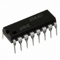
NJM2584D NJR, NJM2584D Datasheet

NJM2584D
Specifications of NJM2584D
Available stocks
Related parts for NJM2584D
NJM2584D Summary of contents
Page 1
... Internal 2 input-1output 3-circuit video switch Operating Current Bipolar Technology Package Outline BLOCK DIAGRAM IN1B NC OUT1 GND2 OUT2 OUT3 NC IN3A 4.5 to 9.0V 50MHz at 0dB typ. 10mA typ. DIP16, DMP16 1 BIAS CLAMP 7 8 NJM2584 PACKAGE OUTLINE NJM2584D NJM2584M 16 IN1A 15 GND1 14 IN2B BIAS CTL 11 IN2A 10 GND3 9 IN3B - 1 - ...
Page 2
NJM2584 ABSOLUTE MAXIMUM RATINGS PARAMETERS Supply Voltage Power Dissipation Operating Temperature Range Storage Temperature Range ELECTRICAL CHARACTERISTICS PARAMETER SYMBOL Operating Current Maximum input Voltage1 Maximum input Voltage 2 Maximum Output Voltage 1 Maximum Output Voltage 2 Voltage Gain Differential Gain ...
Page 3
EQUIVALENT CIRCUIT (V+=5.0V) PIN No. PIN NAME IN1A 16 IN1A IN1B 1 IN1B IN2A 11 IN2A 14 IN2B IN2B 8 IN3A IN3A 9 IN3B IN3B 3 OUT1 5 OUT2 6 OUT3 12 CTL GND1 4 GND2 10 ...
Page 4
NJM2584 TEST CIRCUIT1 75Ω 50Ω 0.1uF 16 15 IN1A GND IN1B 0.1uF 75Ω 50Ω TEST CIRCUIT2 (DG, DP, S/N) 75Ω 50Ω 0.1uF 47uF 47uF + 16 15 IN1A GND IN1B 0.1uF 47uF 47uF ...
Page 5
APPLICATION CIRCUIT 5V 10µF + Yin 10µF + Yin 10µ Uin CTL NJM2584 13 10µF + Uin 10µ Vin A 75 ...
Page 6
NJM2584 TYPICAL CHARACTERISTICS Voltage Gain vs. Frequency 1Vpp sinewave signal input 10 0 -10 -20 1ch-A 1ch-B 2ch-A 2ch-B 3ch-A 3ch-B - 100 Frequency (Hz) Maximum Input Voltage Swing vs. Supply Voltage (BIAS ...
Page 7
Voltage Gain vs. Supply Voltage 2Vpp, 1MHz sinewave signal input 1.0 0.5 0.0 -0.5 -1.0 3.0 4.0 5.0 6.0 7.0 8.0 + Supply Voltage V Channel Gain Defference vs. Supply Voltage 1.0 0.5 0.0 -0.5 -1.0 3.0 4.0 5.0 6.0 ...
Page 8
NJM2584 Input Cross Talk 2 vs. Supply Voltage 2Vpp, 50MHz sinewave signal input (Achannel) -30.0 CTL=H (B Select) -40.0 -50.0 -60.0 -70.0 -80.0 -90.0 3.0 4.0 5.0 6.0 7.0 Supply Voltage V Block Cross Talk 1 vs. Supply Voltage 2Vpp, ...
Page 9
Differential Gain vs. Supply Voltage 1Vpp, 10step video signal input 1.0 0.8 0.6 0.4 0.2 0.0 3.0 4.0 5.0 6.0 7.0 8.0 Supply Voltage V Signal to Noise Ratio vs. Supply Voltage 1Vpp, 100% white video signal input 90.0 85.0 ...
Page 10
NJM2584 APPLICATION This IC requires 1M resistance between INPUT and GND pin for clamp type input since the minute current causes an unstable pin voltage. + Input r This IC requires 0.1uF capacitor between INPUT and GND, 1M type input ...


