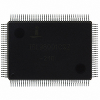
ISL98001CQZ-210 Intersil, ISL98001CQZ-210 Datasheet - Page 11

ISL98001CQZ-210
Manufacturer Part Number
ISL98001CQZ-210
Description
IC TRPL VIDEO DIGITIZER 128-MQFP
Manufacturer
Intersil
Type
Video Digitizerr
Datasheet
1.ISL98001IQZ-140.pdf
(31 pages)
Specifications of ISL98001CQZ-210
Applications
Digital TV, Displays, Digital KVM, Graphics Processing
Mounting Type
Surface Mount
Package / Case
128-MQFP, 128-PQFP
Lead Free Status / RoHS Status
Lead free / RoHS Compliant
Available stocks
Company
Part Number
Manufacturer
Quantity
Price
Company:
Part Number:
ISL98001CQZ-210
Manufacturer:
ICSI
Quantity:
1 025
Part Number:
ISL98001CQZ-210
Manufacturer:
INTERSIL
Quantity:
20 000
Pin Descriptions
HSYNC
VSYNC
V
VREG
SYMBOL
V
VREG
COREADC
V
VS
GND
GND
GND
BYPASS
V
CORE
NC
V
V
V
PLL
OUT
A
D
X
OUT
OUT
OUT
A
D
X
IN
6, 11, 18, 20, 29,
MQFP PIN #(s)
3, 5, 8, 10, 15,
17, 21, 23, 27,
54, 67, 77, 89,
32, 43, 51, 53,
66, 76, 78, 88,
98, 108, 110,
99, 111, 124
52, 79, 109
120, 123
4, 9, 16
1, 2, 63
30, 36
126
127
128
35
38
37
65
64
31
42
(Continued)
11
3.3V digital output. Artificial VSYNC output aligned with pixel data. VS
the trailing edge of HS
3.3V digital output. Buffered HSYNC (or SOG or CSYNC) output. This is typically used for measuring HSYNC
period. This output will pass composite sync signals and Macrovision signals if present on HSYNC
SOG
3.3V digital output. Buffered VSYNC output. For composite sync signals, this output will be asserted for the
duration of the disruption of the normal HSYNC pattern. This is typically used for measuring VSYNC period.
Power supply for the analog section. Connect to a 3.3V supply and bypass each pin to GND
Ground return for V
Power supply for all digital I/Os. Connect to a 3.3V supply and bypass each pin to GND
Ground return for V
Power supply for crystal oscillator. Connect to a 3.3V supply and bypass to GND
Ground return for V
Bypass these pins to GND
3.3V input voltage for V
Regulated output voltage for V
V
else - this output can only supply power to V
Internal power for the ADC’s digital logic. Connect to VREG
with 0.1µF.
Internal power for the PLL’s digital logic. Connect to VREG
with 0.1µF.
Internal power for core logic. Connect to VREG
Reserved. Do not connect anything to these pins.
COREADC
IN
.
and V
CORE
A
D
X
, V
.
and V
OUT
CORE
CORE
and bypass at input pins as instructed in the following. Do not connect to anything
. This signal is usually not needed.
A
BYPASS
ISL98001
with 0.1µF. Do not connect these pins to each other or anything else.
, V
voltage regulator. Connect to a 3.3V source and bypass to GND
PLL
COREADC
, V
.
COREADC
, and V
PLL
DESCRIPTION
OUT
and V
, V
PLL
COREADC
and bypass each pin to GND
.
CORE
OUT
OUT
; typically 1.9V. Connect only to V
and V
through a 10Ω resistor and bypass to GND
through a 10Ω resistor and bypass to GND
CORE
OUT
.
is generated 8 pixel clocks after
X
D
with 0.1µF.
with 0.1µF.
D
with 0.1µF.
A
September 21, 2010
PLL
with 0.1µF.
D
with 0.1µF.
,
IN
FN6148.5
or
D
D


