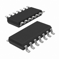
74HCT125D,653 NXP Semiconductors, 74HCT125D,653 Datasheet - Page 3

74HCT125D,653
Manufacturer Part Number
74HCT125D,653
Description
IC BUFFER DVR TRI-ST QD 14SOICN
Manufacturer
NXP Semiconductors
Series
74HCTr
Datasheets
1.74HCT4046ADB112.pdf
(19 pages)
2.74HCT4046ADB112.pdf
(23 pages)
3.74HCT125D653.pdf
(6 pages)
Specifications of 74HCT125D,653
Logic Type
Buffer/Line Driver, Non-Inverting
Package / Case
14-SOIC (3.9mm Width), 14-SOL
Number Of Elements
4
Number Of Bits Per Element
1
Current - Output High, Low
6mA, 6mA
Voltage - Supply
4.5 V ~ 5.5 V
Mounting Type
Surface Mount
Logic Family
74HCT
Number Of Channels Per Chip
4
Polarity
Non-Inverting
Supply Voltage (max)
5.5 V
Supply Voltage (min)
4.5 V
Maximum Operating Temperature
125 C
Mounting Style
SMD/SMT
High Level Output Current
- 6 mA
Input Bias Current (max)
8 uA
Low Level Output Current
6 mA
Maximum Power Dissipation
500 mW
Minimum Operating Temperature
- 40 C
Number Of Lines (input / Output)
8 / 4
Output Type
3-State
Propagation Delay Time
12 ns
Logical Function
Buffer/Line Driver
Number Of Elements
4
Number Of Channels
4
Number Of Inputs
4
Number Of Outputs
4
Operating Supply Voltage (typ)
5V
Package Type
SOIC
Operating Supply Voltage (max)
5.5V
Operating Supply Voltage (min)
4.5V
Quiescent Current
8uA
Technology
CMOS
Pin Count
14
Mounting
Surface Mount
Operating Temp Range
-40C to 125C
Operating Temperature Classification
Automotive
Lead Free Status / RoHS Status
Lead free / RoHS Compliant
Operating Temperature
-
Lead Free Status / Rohs Status
Compliant
Other names
568-1509-2
74HCT125D-T
933757010653
74HCT125D-T
933757010653
Available stocks
Company
Part Number
Manufacturer
Quantity
Price
Philips Semiconductors
RECOMMENDED OPERATING CONDITIONS FOR 74HCU
RATINGS
Limiting values in accordance with the Absolute Maximum System (IEC 134)
Voltages are referenced to GND (ground = 0 V)
Note
1. For analog switches, e.g. “4016”, “4051 series”, “4351 series”, “4066” and “4067”, the specified maximum operating
March 1988
SYMBOL
V
V
V
T
T
SYMBOL
V
T
P
I
I
I
I
I
amb
amb
stg
CC
I
O
CC
tot
HCMOS family characteristics
IK
OK
O
CC
GND
supply voltage is 11 V.
;
PARAMETER
DC supply voltage
DC input diode current
DC output diode current
DC output source or sink
current
DC V
types with:
storage temperature range
power dissipation per package
PARAMETER
DC supply voltage
DC input voltage range
DC output voltage range
operating ambient temperature range
operating ambient temperature range
standard outputs
bus driver outputs
standard outputs
bus driver outputs
plastic DIL
plastic mini-pack (SO)
CC
or GND current for
MIN. MAX. UNIT CONDITIONS
0.5
65
20
20
25
35
50
70
750
500
7
150
3
V
mA
mA
mA
mA
mA
mA
mW
mW
C
for V
for V
for 0.5 V
for temperature range: 40 to 125 C
74HC/HCT/HCU
above 70 C: derate linearly with 12 mW/K
above 70 C: derate linearly with 8 mW/K
min. typ. max.
2.0
0
0
40
40
I
O
74HCU
FAMILY SPECIFICATIONS
5.0
0.5 or V
0.5 or V
V
6.0
V
V
O
85
125
CC
CC
I
V
O
CC
V
V
V
V
UNIT CONDITIONS
C
C
CC
V
CC
0.5 V
0.5 V
see DC and AC
CHAR. per device
0.5 V


