74VCXH245MNR2G ON Semiconductor, 74VCXH245MNR2G Datasheet
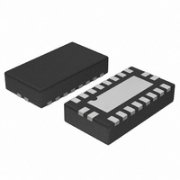
IC TXRX 8BIT 3STATE BIDIR 20QFN

74VCXH245MNR2G

Manufacturer Part Number
74VCXH245MNR2G
Description
IC TXRX 8BIT 3STATE BIDIR 20QFN
Manufacturer
ON Semiconductor
Series
74VCXHr
Datasheet

Specifications of 74VCXH245MNR2G

Logic Type
Transceiver, Non-Inverting
Number Of Elements
1
Number Of Bits Per Element
8
Current - Output High, Low
24mA, 24mA
Voltage - Supply
1.65 V ~ 3.6 V
Operating Temperature
-40°C ~ 85°C
Mounting Type
Surface Mount
Package / Case
20-TFQFN Exposed Pad
Lead Free Status / RoHS Status
Lead free / RoHS Compliant
Other names
74VCXH245MNR2GOS
74VCXH245MNR2GOS
74VCXH245MNR2GOSTR

Available stocks

Company
Part Number
Manufacturer
Quantity
Price
Part Number:
74VCXH245MNR2G
Manufacturer:
ON
Quantity:
42 000
Part Number:
74VCXH245MNR2G
Manufacturer:
BROADCOM
Quantity:
30
74VCXH245
Low−Voltage 1.8/2.5/3.3 V
8−Bit Transceiver
(3−State, Non−Inverting with Bushold)
transceiver. It is designed for very high−speed, very low−power
operation in 1.8 V, 2.5 V or 3.3 V systems.
Transmit/Receive (T/Rn) inputs determine the direction of data flow
through the bidirectional transceiver. Transmit (active−HIGH) enables
data from A ports to B ports; Receive (active−LOW) enables data from
B to A ports. The Output Enable input (OE), when HIGH, disables
both A and B ports by placing them in a HIGH Z condition. The data
inputs include active bushold circuitry, eliminating the need for
external pullup resistors to hold unused or floating inputs at a valid
logic state.
Features
*For additional information on our Pb−Free strategy and soldering details, please
April, 2005 − Rev. 10
download the ON Semiconductor Soldering and Mounting Techniques
Reference Manual, SOLDERRM/D.
The 74VCXH245 is an advanced performance, non−inverting 8−bit
The 74VCXH245 is designed as a byte control. The
Valid Logic State
Substantially Reduces System Power Requirements
ESD Performance:
Designed for Low Voltage Operation: V
High Speed Operation:
Static Drive:
Includes Active Bushold to Hold Unused or Floating Data Inputs at a
Near Zero Static Supply Current in All Three Logic States (20 mA)
Latchup Performance Exceeds 200 mA @ 85 C
Pb−Free Package is Available
Semiconductor Components Industries, LLC, 2005
24 mA Drive at 3.0 V
18 mA Drive at 2.3 V
6 mA Drive at 1.65 V
Human Body Model >2000 V
Machine Model >200 V
3.5 ns max for 3.0 to 3.6 V
4.2 ns max for 2.3 to 2.7 V
8.4 ns max for 1.65 to 1.95 V
CC
= 1.65−3.6 V
1
74VCXH245MNR2G
†For information on tape and reel specifications,
74VCXH245MNR2
PIN #1
including part orientation and tape sizes, please
refer to our Tape and Reel Packaging Specifications
Brochure, BRD8011/D.
20
MNR2 SUFFIX
Device
CASE 485AA
A
L
Y
W
(Note: Microdot may be in either location)
G
ORDERING INFORMATION
19
2
QFN
http://onsemi.com
Pinout (Top View)
= Assembly Location
= Wafer Lot
= Year
= Work Week
= Pb−Free Package
(Pb−Free)
Package
QFN
QFN
QFN
Publication Order Number:
3000/Tape&Reel
3000/Tape&Reel
MARKING
DIAGRAM
74VCXH245/D
ALYWG
Shipping
H245
1
VCX
12
9
G
11
10

Related parts for 74VCXH245MNR2G

74VCXH245MNR2G Summary of contents

Page 1

... Reference Manual, SOLDERRM/D. Semiconductor Components Industries, LLC, 2005 April, 2005 − Rev 1.65−3 PIN #1 74VCXH245MNR2 74VCXH245MNR2G †For information on tape and reel specifications, including part orientation and tape sizes, please refer to our Tape and Reel Packaging Specifications Brochure, BRD8011/D. 1 http://onsemi.com ...

Page 2

PIN NAMES PINS FUNCTION OE Output Enable Input T/R Transmit/Receive Input A0−A7 Side A Bushold Inputs or 3−State Outputs B0−B7 Side B Bushold Inputs or 3−State Outputs TRUTH TABLE INPUTS OPERATING MODE OE T ...

Page 3

RECOMMENDED OPERATING CONDITIONS Symbol V Supply Voltage CC V Input Voltage I V Output Voltage O I HIGH Level Output Current LOW Level Output Current HIGH Level Output Current LOW Level ...

Page 4

DC ELECTRICAL CHARACTERISTICS Symbol Characteristic V HIGH Level Input Voltage (Note LOW Level Input Voltage (Note HIGH Level Output Voltage OH V LOW Level Output Voltage OL I Input Leakage Current I I Minimum ...

Page 5

AC CHARACTERISTICS (Note Symbol Parameter t Propagation Delay PLH t Input to Output PHL t Output Enable Time to PZH t High and Low Level PZL t Output Disable Time From PHZ t High and Low Level ...

Page 6

Vm An PLH Bn, An WAVEFORM 1 − PROPAGATION DELAYS 2.0 ns, 10 MHz OEn, T/Rn t PZH Vm An PZL Vm ...

Page 7

D PIN ONE REFERENCE 2X 0. 0. 0.08 C 20X (A3 20X 20X NOTE 3 74VCXH245 PACKAGE ...

Page 8

... Fax: 480−829−7709 or 800−344−3867 Toll Free USA/Canada Email: orderlit@onsemi.com 74VCXH245 N. American Technical Support: 800−282−9855 Toll Free USA/Canada Japan: ON Semiconductor, Japan Customer Focus Center 2−9−1 Kamimeguro, Meguro−ku, Tokyo, Japan 153−0051 Phone: 81−3−5773−3850 http://onsemi.com 8 ON Semiconductor Website: http://onsemi ...

Related keywords