74VCXH16245DTRG ON Semiconductor, 74VCXH16245DTRG Datasheet
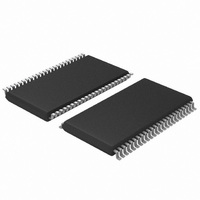
IC TXRX 16BIT CMOS BIDIR 48TSSOP

74VCXH16245DTRG

Manufacturer Part Number
74VCXH16245DTRG
Description
IC TXRX 16BIT CMOS BIDIR 48TSSOP
Manufacturer
ON Semiconductor
Series
74VCXHr
Datasheet

Specifications of 74VCXH16245DTRG

Logic Type
Transceiver, Non-Inverting
Number Of Elements
2
Number Of Bits Per Element
8
Current - Output High, Low
24mA, 24mA
Voltage - Supply
1.65 V ~ 3.6 V
Operating Temperature
-40°C ~ 85°C
Mounting Type
Surface Mount
Package / Case
48-TSSOP
Lead Free Status / RoHS Status
Lead free / RoHS Compliant

Available stocks

Company
Part Number
Manufacturer
Quantity
Price
Part Number:
74VCXH16245DTRG
Manufacturer:
STM
Quantity:
6 186
Part Number:
74VCXH16245DTRG
Manufacturer:
ON/安森美
Quantity:
20 000
74VCXH16245
Low−Voltage 1.8/2.5/3.3V
16−Bit Transceiver
With 3.6 V−Tolerant Inputs and Outputs
(3−State, Non−Inverting)
16−bit transceiver. It is designed for very high−speed, very low−power
operation in 1.8 V, 2.5 V or 3.3 V systems.
voltages it may encounter on either inputs or outputs when interfacing
to 3.3 V busses. It is guaranteed to be over−voltage tolerant to 3.6 V.
as two separate octals, or with the controls tied together, as a 16−bit
wide function. The Transmit/Receive (T/Rn) inputs determine the
direction of data flow through the bi−directional transceiver. Transmit
(active−HIGH) enables data from A ports to B ports; Receive
(active−LOW) enables data from B to A ports. The Output Enable
inputs (OEn), when HIGH, disable both A and B ports by placing them
in a HIGH Z condition. The data inputs include active bushold
circuitry, eliminating the need for external pull−up resistors to hold
unused or floating inputs at a valid logic state.
Features
*NOTE: To ensure the outputs activate in the 3−state condition,
May, 2004 − Rev. 3
the output enable pins should be connected to V
pull−up resistor. The value of the resistor is determined by the
current sinking capability of the output connected to the OE pin.
The 74VCXH16245 is an advanced performance, non−inverting
When operating at 2.5 V (or 1.8 V) the part is designed to tolerate
The VCXH16245 is designed with byte control. It can be operated
Logic State
Substantially Reduces System Power Requirements
ESD Performance: Human Body Model >2000 V;
Designed for Low Voltage Operation: V
3.6 V Tolerant Inputs and Outputs
High Speed Operation: 2.5 ns max for 3.0 to 3.6 V
Static Drive:
Supports Live Insertion and Withdrawal
Includes Active Bushold to Hold Unused or Floating Inputs at a Valid
I
Near Zero Static Supply Current in All Three Logic States (20 mA)
Latchup Performance Exceeds 250 mA @ 125 C
Pb−Free Package is Available*
Semiconductor Components Industries, LLC, 2004
Machine Model >200 V
OFF
Specification Guarantees High Impedance When V
24 mA Drive at 3.0 V
18 mA Drive at 2.3 V
6 mA Drive at 1.65 V
3.0 ns max for 2.3 to 2.7 V
6.0 ns max for 1.65 to 1.95 V
CC
CC
= 1.65−3.6 V
through a
CC
1
= 0 V
*
74VCXH16245DT
74VCXH16245DTR
74VCXH16245DTRG TSSOP
†For information on tape and reel specifications,
*For additional information on our Pb−Free strategy
including part orientation and tape sizes, please
refer to our Tape and Reel Packaging Specification
Brochure, BRD8011/D.
and soldering details, please download the
ON Semiconductor Soldering and Mounting
Techniques Reference Manual, SOLDERRM/D.
48
Device
ORDERING INFORMATION
48
1
A
WL = Wafer Lot
YY = Year
WW = Work Week
MARKING DIAGRAM
1
http://onsemi.com
= Assembly Location
VCXH16245
AWLYYWW
(Pb−Free)
Package
TSSOP
TSSOP
Publication Order Number:
CASE 1201
DT SUFFIX
TSSOP−48
2500/Tape & Reel
2500/Tape & Reel
74VCXH16245/D
Shipping
39 / Rail

Related parts for 74VCXH16245DTRG

74VCXH16245DTRG Summary of contents

Page 1

... May, 2004 − Rev 1.65−3 74VCXH16245DT * = 74VCXH16245DTR 74VCXH16245DTRG TSSOP †For information on tape and reel specifications, including part orientation and tape sizes, please refer to our Tape and Reel Packaging Specification Brochure, BRD8011/D. *For additional information on our Pb−Free strategy through a CC and soldering details, please download the ON Semiconductor Soldering and Mounting Techniques Reference Manual, SOLDERRM/D ...

Page 2

T/ OE1 GND 4 45 GND GND GND 10 ...

Page 3

ABSOLUTE MAXIMUM RATINGS* Symbol Parameter V DC Supply Voltage Input Voltage Output Voltage Input Diode Current Output Diode Current Output Source/Sink Current ...

Page 4

DC ELECTRICAL CHARACTERISTICS Symbol Characteristic V HIGH Level Input Voltage (Note 2 LOW Level Input Voltage (Note 2 HIGH Level Output Voltage OH V LOW Level Output Voltage OL I Input Leakage Current I I Minimum ...

Page 5

AC CHARACTERISTICS (Note 6 Symbol Parameter t Propagation Delay PLH t Input to Output PHL t Output Enable Time to PZH t High and Low Level PZL t Output Disable Time From PHZ t High and Low Level ...

Page 6

Vm An PLH Bn, An WAVEFORM 1 − PROPAGATION DELAYS 2.0ns, 10 1MHz OEn, T/Rn t PZH Vm An PZL Vm An, Bn ...

Page 7

Vm An PLH Bn, An WAVEFORM 3 − PROPAGATION DELAYS 2.0ns, 10 1MHz OEn, T/Rn t PZH An PZL An, Bn WAVEFORM 4 ...

Page 8

... DETAIL E DETAIL American Technical Support: 800−282−9855 Toll Free USA/Canada Japan: ON Semiconductor, Japan Customer Focus Center 2−9−1 Kamimeguro, Meguro−ku, Tokyo, Japan 153−0051 Phone: 81−3−5773−3850 http://onsemi.com 8 NOTES: 1. DIMENSIONING AND TOLERANCING PER ANSI Y14.5M, 1982. ...

Related keywords