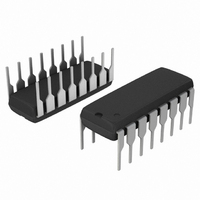
MC74HC4040ANG ON Semiconductor, MC74HC4040ANG Datasheet - Page 4

MC74HC4040ANG
Manufacturer Part Number
MC74HC4040ANG
Description
IC COUNTER RIPPLE 12STAGE 16DIP
Manufacturer
ON Semiconductor
Series
74HCr
Specifications of MC74HC4040ANG
Logic Type
Binary Counter
Direction
Up
Number Of Elements
1
Number Of Bits Per Element
12
Reset
Asynchronous
Count Rate
50MHz
Trigger Type
Negative Edge
Voltage - Supply
2 V ~ 6 V
Operating Temperature
-55°C ~ 125°C
Mounting Type
Through Hole
Package / Case
16-DIP (0.300", 7.62mm)
Counter Type
Binary
Counting Sequence
Up
Number Of Circuits
1
Logic Family
74HC
Propagation Delay Time
96 ns, 63 ns, 31 ns, 25 ns
Supply Voltage (max)
6 V
Maximum Operating Temperature
+ 125 C
Minimum Operating Temperature
- 55 C
Function
Counter
Mounting Style
Through Hole
Operating Supply Voltage
2 V to 6 V
Circuit Type
Silicon Gate
Current, Supply
160 μA
Function Type
12-Stages
Logic Function
Counter
Package Type
PDIP-16
Special Features
Binary, Ripple
Temperature, Operating, Range
-55 to +125 °C
Voltage, Supply
2 to 6 V
Lead Free Status / RoHS Status
Lead free / RoHS Compliant
Timing
-
Lead Free Status / Rohs Status
Lead free / RoHS Compliant
Other names
MC74HC4040ANGOS
Available stocks
Company
Part Number
Manufacturer
Quantity
Price
Company:
Part Number:
MC74HC4040ANG
Manufacturer:
ON Semiconductor
Quantity:
1 949
Company:
Part Number:
MC74HC4040ANG
Manufacturer:
ON Semiconductor
Quantity:
2 350
* For T
* Used to determine the no−load dynamic power consumption: P
DC CHARACTERISTICS
AC CHARACTERISTICS
Symbol
Symbol
Symbol
t
t
t
t
t
t
f
t
C
PLH
PLH
TLH
I
max
PHL
PHL
PHL
THL
C
I
CC
in
PD
in
,
,
,
V
V
A
CC
CC
= 25°C and C
= 2.0 V: t
= 3.0 V: t
Maximum Input Leakage Current
Maximum Quiescent Supply
Current (per Package)
Maximum Clock Frequency (50% Duty Cycle)
(Figures 1 and 4)
Maximum Propagation Delay, Clock to Q1*
(Figures 1 and 4)
Maximum Propagation Delay, Reset to Any Q
(Figures 2 and 4)
Maximum Propagation Delay, Qn to Qn+1
(Figures 3 and 4)
Maximum Output Transition Time, Any Output
(Figures 1 and 4)
Maximum Input Capacitance
Power Dissipation Capacitance (Per Package)*
P
P
= [93.7 + 59.3 (n−1)] ns
= [61.5 + 34.4 (n−1)] ns
L
Parameter
Parameter
= 50 pF, typical propagation delay from Clock to other Q outputs may be calculated with the following equations:
(Voltages Referenced to GND)
(C
L
= 50 pF, Input t
Parameter
r
= t
V
V
V
I
out
in
in
in
f
= 6 ns)
= V
= V
= V
= 0mA
IH
CC
CC
http://onsemi.com
or V
or GND
or GND
Condition
Condition
V
V
IL
CC
CC
D
= 4.5 V: t
= 6.0V: t
4
= C
|I
|I
|I
out
out
out
PD
| ≤ 2.4mA
| ≤ 4.0mA
| ≤ 5.2mA
P
V
P
CC
= [24.4 + 12 (n−1)] ns
= [30.25 + 14.6 (n−1)] ns
2
f + I
CC
V
V
V
3.0
4.5
6.0
6.0
6.0
2.0
3.0
4.5
6.0
2.0
3.0
4.5
6.0
2.0
3.0
4.5
6.0
2.0
3.0
4.5
6.0
2.0
3.0
4.5
6.0
V
V
V
V
CC
CC
CC
CC
.
−55 to 25°C
−55 to 25°C
Typical @ 25°C, V
0.26
0.26
0.26
±0.1
10
15
30
50
96
63
31
25
65
30
30
26
69
40
17
14
75
27
15
13
10
4
Guaranteed Limit
Guaranteed Limit
31
≤85°C
≤85°C
0.33
0.33
0.33
±1.0
106
9.0
40
14
28
45
71
36
30
72
36
35
32
80
45
21
15
95
32
19
15
10
CC
= 5.0 V
≤125°C
≤125°C
0.40
0.40
0.40
±1.0
160
115
110
8.0
12
25
40
88
40
35
90
40
40
35
90
50
28
22
36
22
19
10
MHz
Unit
Unit
Unit
mA
mA
pF
pF
ns
ns
ns
ns


