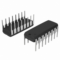
MC74HC4040ANG ON Semiconductor, MC74HC4040ANG Datasheet - Page 5

MC74HC4040ANG
Manufacturer Part Number
MC74HC4040ANG
Description
IC COUNTER RIPPLE 12STAGE 16DIP
Manufacturer
ON Semiconductor
Series
74HCr
Specifications of MC74HC4040ANG
Logic Type
Binary Counter
Direction
Up
Number Of Elements
1
Number Of Bits Per Element
12
Reset
Asynchronous
Count Rate
50MHz
Trigger Type
Negative Edge
Voltage - Supply
2 V ~ 6 V
Operating Temperature
-55°C ~ 125°C
Mounting Type
Through Hole
Package / Case
16-DIP (0.300", 7.62mm)
Counter Type
Binary
Counting Sequence
Up
Number Of Circuits
1
Logic Family
74HC
Propagation Delay Time
96 ns, 63 ns, 31 ns, 25 ns
Supply Voltage (max)
6 V
Maximum Operating Temperature
+ 125 C
Minimum Operating Temperature
- 55 C
Function
Counter
Mounting Style
Through Hole
Operating Supply Voltage
2 V to 6 V
Circuit Type
Silicon Gate
Current, Supply
160 μA
Function Type
12-Stages
Logic Function
Counter
Package Type
PDIP-16
Special Features
Binary, Ripple
Temperature, Operating, Range
-55 to +125 °C
Voltage, Supply
2 to 6 V
Lead Free Status / RoHS Status
Lead free / RoHS Compliant
Timing
-
Lead Free Status / Rohs Status
Lead free / RoHS Compliant
Other names
MC74HC4040ANGOS
Available stocks
Company
Part Number
Manufacturer
Quantity
Price
Company:
Part Number:
MC74HC4040ANG
Manufacturer:
ON Semiconductor
Quantity:
1 949
Company:
Part Number:
MC74HC4040ANG
Manufacturer:
ON Semiconductor
Quantity:
2 350
INPUTS
Clock (Pin 10)
transition on this input advances the state of the counter.
Reset (Pin 11)
asynchronously resets the counter to its zero state, thus
forcing all Q outputs low.
TIMING REQUIREMENTS
Symbol
Negative−edge triggering clock input. A high−to−low
Active−high reset. A high level applied to this input
t
t
r
rec
t
t
, t
w
w
Clock
f
Q1
Minimum Recovery Time, Reset Inactive to Clock
(Figure 2)
Minimum Pulse Width, Clock
(Figure 1)
Minimum Pulse Width, Reset
(Figure 2)
Maximum Input Rise and Fall Times
(Figure 1)
10%
50%
90%
90%
50%
10%
t
f
t
t
PLH
w
t
TLH
Figure 3.
(Input t
1/f
MAX
r
= t
t
r
f
t
PHL
= 6 ns)
Parameter
t
THL
SWITCHING WAVEFORMS
PIN DESCRIPTIONS
http://onsemi.com
V
GND
CC
5
OUTPUTS
Q1 thru Q12 (Pins 9, 7, 6, 5, 3, 2, 4, 13, 12, 14, 15, 1)
input frequency by 2
Active−high outputs. Each Qn output divides the Clock
Any Q
Reset
Clock
2.0
3.0
4.5
6.0
V
2.0
3.0
4.5
6.0
2.0
3.0
4.5
6.0
2.0
3.0
4.5
6.0
V
CC
N
−55 to 25°C
.
1000
Figure 4.
800
500
400
30
20
70
40
15
13
70
40
15
13
5
4
Guaranteed Limit
t
PHL
50%
t
≤85°C
w
1000
800
500
400
t
40
25
80
45
19
16
80
45
19
16
rec
8
6
50%
50%
≤125°C
1000
800
500
400
50
30
12
90
50
24
20
90
50
24
20
9
V
GND
V
GND
Unit
CC
CC
ns
ns
ns
ns


