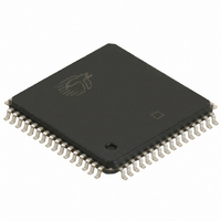
CY7C4255-10AC Cypress Semiconductor Corp, CY7C4255-10AC Datasheet - Page 18

CY7C4255-10AC
Manufacturer Part Number
CY7C4255-10AC
Description
IC DEEP SYNC FIFO 8KX18 64LQFP
Manufacturer
Cypress Semiconductor Corp
Series
CY7Cr
Specifications of CY7C4255-10AC
Function
Synchronous
Memory Size
144K (8K x 18)
Data Rate
100MHz
Access Time
8ns
Voltage - Supply
3.3V
Operating Temperature
-40°C ~ 85°C
Mounting Type
Surface Mount
Package / Case
64-LQFP
Configuration
Dual
Density
144Kb
Access Time (max)
8ns
Word Size
18b
Organization
8Kx18
Sync/async
Synchronous
Expandable
Yes
Bus Direction
Uni-Directional
Package Type
TQFP
Clock Freq (max)
100MHz
Operating Supply Voltage (typ)
5V
Operating Supply Voltage (min)
4.5V
Operating Supply Voltage (max)
5.5V
Supply Current
45mA
Operating Temp Range
0C to 70C
Operating Temperature Classification
Commercial
Mounting
Surface Mount
Pin Count
64
Lead Free Status / RoHS Status
Contains lead / RoHS non-compliant
Other names
428-1230
Available stocks
Company
Part Number
Manufacturer
Quantity
Price
Company:
Part Number:
CY7C4255-10AC
Manufacturer:
Cypress Semiconductor Corp
Quantity:
10 000
Depth Expansion Configuration
(with Programmable Flags)
The CY7C4255/65 can easily be adapted to applications re-
quiring more than 8192/16384 words of buffering. Figure 2
shows Depth Expansion using three CY7C42X5s. Maximum depth
is limited only by signal loading. Follow these steps:
Document #: 38-06004 Rev. *A
1. The first device must be designated by grounding the First
2. All other devices must have FL in the HIGH state.
DATA IN(D)
Load (FL) control input.
LOAD (LD)
FF
PAF
Figure 2. Block Diagram of 8Kx18/16Kx18 Synchronous FIFO Memory
WRITE CLOCK(WCLK)
WRITE ENABLE(WEN)
RESET (RS)
with Programmable Flags used in Depth Expansion Configuration
FIRST LOAD (FL)
V
V
CC
CC
FF
PAF
FF
PAF
FF
PAF
FL
FL
WXO RXO
WXO RXO
WXO RXO
7C4255
7C4265
WXI RXI
7C4255
7C4265
WXI RXI
7C4255
7C4265
WXI RXI
3. The Write Expansion Out (WXO) pin of each device must be
4. The Read Expansion Out (RXO) pin of each device must be
5. All Load (LD) pins are tied together.
6. The Half-Full Flag (HF) is not available in the Depth Expansion
7. EF, FF, PAE, and PAF are created with composite flags by
PAE
PAE
PAE
EF
EF
EF
tied to the Write Expansion In (WXI) pin of the next device.
tied to the Read Expansion In (RXI) pin of the next device.
Configuration.
ORing together these respective flags for monitoring. The
composite PAE and PAF flags are not precise.
READ CLOCK(RCLK)
READ ENABLE(REN)
OUTPUT ENABLE(OE)
4255–25
PAE
EF
DATA OUT (Q)
CY7C4255
CY7C4265
Page 18 of 22


