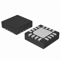
NB4L52MNR2G ON Semiconductor, NB4L52MNR2G Datasheet - Page 2

NB4L52MNR2G
Manufacturer Part Number
NB4L52MNR2G
Description
IC FLIP FLOP DATA/CLK DFF 16-QFN
Manufacturer
ON Semiconductor
Type
D-Typer
Datasheet
1.NB4L52MNR2G.pdf
(8 pages)
Specifications of NB4L52MNR2G
Function
Reset
Output Type
Differential
Number Of Elements
1
Number Of Bits Per Element
1
Delay Time - Propagation
400ps
Trigger Type
Negative Edge
Voltage - Supply
2.3 V ~ 5.5 V
Operating Temperature
-40°C ~ 85°C
Mounting Type
Surface Mount
Package / Case
16-TQFN Exposed Pad
Lead Free Status / RoHS Status
Lead free / RoHS Compliant
Current - Output High, Low
-
Frequency - Clock
-
1. In the differential configuration when the input termination pin (VTD, VTD, VTR, VTR, VTCLK, VTCLK) are connected to a common
Table 2. PIN DESCRIPTION
Pin
10
11
12
13
14
15
16
1
2
3
4
5
6
7
8
9
−
termination voltage or left open, and if no signal is applied on D/D,CLK/CLK,R/R input then the device will be susceptible to self−oscillation.
Name
V
V
CLK
CLK
V
V
V
V
V
V
TCLK
TCLK
EP
Q
Q
D
D
R
R
CC
TD
TD
EE
TR
TR
ECL, CML, LVCMOS,
ECL, CML, LVCMOS,
ECL, CML, LVCMOS,
ECL, CML, LVCMOS,
LVDS, LVTTL Input
LVDS, LVTTL Input
LVDS, LVTTL Input
LVDS, LVTTL Input
LVECL, LVCMOS,
LVECL, LVCMOS,
LVTTL Input
LVTTL Input
ECL Output
ECL Output
I/O
−
−
−
−
−
−
−
−
−
V
V
TD
TD
D
D
Internal 50 W Termination Pin. (See Table 4)
Noninverted Differential Input. (Note 1)
Inverted Differential Input. (Note 1)
Internal 50 W Termination Pin. (See Table 4)
Internal 50 W Termination Pin. (See Table 4)
Noninverted Differential Input. (Note 1)
Inverted Differential Input. (Note 1)
Internal 50 W Termination Pin. (See Table 4)
Negative Supply Voltage
Inverted Differential Output. Typically terminated with 50 W resistor to V
Noninverted Differential Output. Typically terminated with 50 W resistor to V
Positive Supply Voltage
Internal 50 W Termination Pin. (See Table 4)
Noninverted Differential Reset Input. (Note 1)
Inverted Differential Reset Input. (Note 1)
Internal 50 W Termination Pin. (See Table 4)
The Exposed Pad (EP) on the QFN−16 package bottom is thermally connected to the die
for improved heat transfer out of package. The pad is not electrically connected to the die,
but is recommended to be electrically and thermally connected to V
1
2
3
4
Figure 2. Pinout (Top View)
V
V
TCLK
16
http://onsemi.com
5
TR
CLK
15
R
6
NB4L52
2
CLK
14
R
7
V
V
TCLK
13
8
TR
Exposed Pad (EP)
Description
12
10
11
9
V
Q
Q
V
CC
EE
EE
on the PC board.
CC
− 2.0 V.
CC
− 2.0 V.


