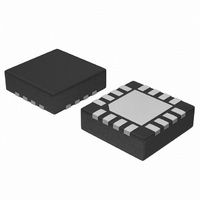
NB4L52MNR2G ON Semiconductor, NB4L52MNR2G Datasheet - Page 5

NB4L52MNR2G
Manufacturer Part Number
NB4L52MNR2G
Description
IC FLIP FLOP DATA/CLK DFF 16-QFN
Manufacturer
ON Semiconductor
Type
D-Typer
Datasheet
1.NB4L52MNR2G.pdf
(8 pages)
Specifications of NB4L52MNR2G
Function
Reset
Output Type
Differential
Number Of Elements
1
Number Of Bits Per Element
1
Delay Time - Propagation
400ps
Trigger Type
Negative Edge
Voltage - Supply
2.3 V ~ 5.5 V
Operating Temperature
-40°C ~ 85°C
Mounting Type
Surface Mount
Package / Case
16-TQFN Exposed Pad
Lead Free Status / RoHS Status
Lead free / RoHS Compliant
Current - Output High, Low
-
Frequency - Clock
-
Table 6. AC CHARACTERISTICS
NOTE: Device will meet the specifications after thermal equilibrium has been established when mounted in a test socket or printed circuit
8. Measured by forcing V
9. Additive RMS jitter with 50% duty cycle clock signal.
10. Input and output voltage swing is a single−ended measurement operating in differential mode.
Symbol
V
t
t
t
t
t
t
t
V
t
t
PLH
PHL
s
h
RR
PW
JITTER
r
f
OUTPP
INPP
rates 40 ps (20% − 80%).
,
board with maintained transverse airflow greater than 500 lfpm. Electrical parameters are guaranteed only over the declared
operating temperature range. Functional operation of the device exceeding these conditions is not implied. Device specification
limit values are applied individually under normal operating conditions and not valid simultaneously.
Output Voltage Amplitude (@ V
Propagation Delay to
Output Differential
Setup Time
Hold Time
Reset Recovery
Minimum Pulse Width
RMS Random Clock Jitter (Note 9)
Input Voltage Swing/Sensitivity
(Differential Configuration) (Note 10)
Output Rise/Fall Times @ 0.5 GHz
(20% − 80%)
(Note 10) (See Figure 4)
INPP
800
700
600
500
400
300
200
100
Characteristic
(MIN) from a 50% duty cycle clock source. All loading with an external R
0
0
Clock Input Frequency at Ambient Temperature (Typical).
V
Figure 3. Output Voltage Amplitude (V
CC
INPPmin
= 2.375 V to 5.5 V; V
CLK to Q, R to Q
f
f
f
f
f
f
in
in
in
in
in
in
f
in
)
1
v 2.0 GHz
v 3.0 GHz
v 4.0 GHz
v 2.0 GHz
v 3.0 GHz
v 4.0 GHz
, CLOCK INPUT FREQUENCY (GHz)
http://onsemi.com
R/R
Min
EE
530
490
380
300
100
400
250
150
50
80
5
= 0 V or V
2
−40°C
Typ
770
720
580
400
135
1
1
1
CC
2800
Max
500
190
= 0 V, V
OUTPP
3
Min
530
490
380
300
100
400
250
150
50
80
EE
) vs.
= −2.375 to −5.5 V (Note 8)
25°C
Typ
780
730
580
400
145
1
1
1
L
2800
Max
500
190
= 50 W to V
4
Min
530
490
380
300
100
400
250
150
50
80
CC
85°C
– 2.0 V. Input edge
Typ
760
680
530
400
155
1
1
1
2800
Max
500
190
Unit
mV
mV
ps
ps
ps
ps
ps
ps
ps


