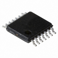
74LVT00PW,112 NXP Semiconductors, 74LVT00PW,112 Datasheet - Page 3

74LVT00PW,112
Manufacturer Part Number
74LVT00PW,112
Description
IC QUAD 2-IN NAND GATE 14-TSSOP
Manufacturer
NXP Semiconductors
Series
74LVTr
Datasheet
1.74LVT00PW118.pdf
(10 pages)
Specifications of 74LVT00PW,112
Number Of Circuits
4
Package / Case
14-TSSOP
Logic Type
NAND Gate
Number Of Inputs
2
Current - Output High, Low
20mA, 32mA
Voltage - Supply
2.7 V ~ 3.6 V
Operating Temperature
-40°C ~ 85°C
Mounting Type
Surface Mount
Product
NAND
Logic Family
74LVT
Propagation Delay Time
2.7 ns
Maximum Operating Temperature
85 C
Mounting Style
SMD/SMT
Minimum Operating Temperature
-40 C
Lead Free Status / RoHS Status
Lead free / RoHS Compliant
Lead Free Status / RoHS Status
Lead free / RoHS Compliant, Lead free / RoHS Compliant
Other names
568-3024-5
935208940112
935208940112
1. Stresses beyond those listed may cause permanent damage to the device. These are stress ratings only and functional operation of the
2. The performance capability of a high-performance integrated circuit in conjunction with its thermal environment can create junction
3. The input and output negative voltage ratings may be exceeded if the input and output clamp current ratings are observed.
Philips Semiconductors
LOGIC DIAGRAM
ABSOLUTE MAXIMUM RATINGS
NOTES:
RECOMMENDED OPERATING CONDITIONS
1996 Aug 15
V
GND = Pin 7
SYMBOL
SYMBOL
SYMBOL
CC
3.3V Quad 2-input NAND gate
device at these or any other conditions beyond those indicated under “recommended operating conditions” is not implied. Exposure to
absolute-maximum-rated conditions for extended periods may affect device reliability.
temperatures which are detrimental to reliability. The maximum junction temperature of this integrated circuit should not exceed 150 C.
V
T
I
I
V
V
T
I
OUT
V
I
= Pin 14
V
I
I
OUT
t/ v
amb
V
OK
V
OH
OL
CC
IK
stg
CC
IH
IL
I
I
DC supply voltage
DC input diode current
DC input voltage
DC output diode current
DC output voltage
DC output current
DC output current
Storage temperature range
DC supply voltage
Input voltage
High-level input voltage
Low-level Input voltage
High-level output current
Low-level output current
Input transition rise or fall rate; Outputs enabled
Operating free-air temperature range
A0
B0
A1
B1
A2
B2
A3
B3
10
12
13
1
2
4
5
9
PARAMETER
3
3
3
6
8
11
1, 2
SA00360
Y3
Y0
Y1
Y2
PARAMETER
PARAMETER
Output in Off or High state
3
Output in High state
Output in Low state
H = High voltage level
L = Low voltage level
CONDITIONS
FUNCTION TABLE
NOTES:
V
V
O
I
Dna
< 0
< 0
H
H
L
L
INPUTS
Dnb
H
H
L
L
MIN
–40
2.7
2.0
0
–0.5 to +4.6
–0.5 to +7.0
–0.5 to +7.0
–65 to 150
RATING
LIMITS
–50
–50
–32
64
MAX
–20
+85
3.6
5.5
0.8
32
10
OUTPUT
Product specification
74LVT00
Qn
H
H
L
H
UNIT
UNIT
UNIT
ns/V
mA
mA
mA
mA
mA
mA
V
V
V
V
V
V
V
C
C


