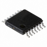
74LVT00PW,112 NXP Semiconductors, 74LVT00PW,112 Datasheet - Page 4

74LVT00PW,112
Manufacturer Part Number
74LVT00PW,112
Description
IC QUAD 2-IN NAND GATE 14-TSSOP
Manufacturer
NXP Semiconductors
Series
74LVTr
Datasheet
1.74LVT00PW118.pdf
(10 pages)
Specifications of 74LVT00PW,112
Number Of Circuits
4
Package / Case
14-TSSOP
Logic Type
NAND Gate
Number Of Inputs
2
Current - Output High, Low
20mA, 32mA
Voltage - Supply
2.7 V ~ 3.6 V
Operating Temperature
-40°C ~ 85°C
Mounting Type
Surface Mount
Product
NAND
Logic Family
74LVT
Propagation Delay Time
2.7 ns
Maximum Operating Temperature
85 C
Mounting Style
SMD/SMT
Minimum Operating Temperature
-40 C
Lead Free Status / RoHS Status
Lead free / RoHS Compliant
Lead Free Status / RoHS Status
Lead free / RoHS Compliant, Lead free / RoHS Compliant
Other names
568-3024-5
935208940112
935208940112
1. All typical values are at V
2. This is the increase in supply current for each input at the specificed voltage level other than V
1. All typical values are at V
Philips Semiconductors
DC ELECTRICAL CHARACTERISTICS
Over recommended operating conditions
Voltages are referenced to GND (ground = 0V)
NOTES:
AC CHARACTERISTICS
GND = 0V; t
NOTE:
AC WAVEFORMS
V
1996 Aug 15
SYMBOL
M
SYMBOL
3.3V Quad 2-input NAND gate
= 1.5V, V
I
V
I
I
V
V
CCH
OFF
CCL
C
I
t
t
Waveform 1. Propagation delay for inverting outputs
OH
OL
I
I
CC
IK
PLH
PHL
I
A
I
n
, B
Yn
n
R
IN
= t
= GND to 2.7V
Input clamp voltage
High-level output voltage
Low-level output voltage
Input leakage current
Input leakage current
Output off current
Quiescent supply current
Quiescent supply current
Additional supply current per input pin
Input capacitance
F
Propagation delay
An or Bn to Yn
= 2.5ns; C
V
M
CC
CC
t
PARAMETER
L
PARAMETER
PHL
= 50pF, R
V
= 3.3V and T
= 3.3V and T
M
V
M
L
= 500 ; T
amb
amb
t
PLH
= 25 C.
= 25 C.
V
M
amb
2
= –40 C to +85 C.
SF01395
V
V
V
V
V
V
V
V
V
V
V
V
V
I
V
Other inputs at V
V
O =
CC
CC
CC
CC
CC
CC
CC
CC
CC
CC
CC
CC,
CC
CC
I
= 3V or 0
WAVEFORM
0
= 2.7V; I
= 2.7 to 3.6V; I
= 2.7V; I
= 3.0V; I
= 2.7V; I
= 2.7V; I
= 3.0V; I
= 0 or 3.6V; V
= 3.6V; V
= 0V; V
= 3.6V; Outputs High, V
= 3.6V; Outputs Low, V
= 3V to 3.6V; One input at V
I
O =
0
1
4
TEST CONDITIONS
I
IK
OH
OH
OL
OL
OL
or V
I
= V
= –18mA
= 100 A
= 24mA
= 32mA
= –6mA
= –20mA
CC
O
I
CC
OH
= 0 to 4.5V
= 5.5V
or GND
or GND
= –100 A
MIN
1.0
1.0
I
I
= GND or V
= GND or
V
CC
CC
–0.6V,
= 3.3V
CC
TYP
2.7
2.7
or GND.
CC,
1
LIMITS
0.3V
V
Temp = -40 C to +85 C
CC
MIN
MAX
2.4
2.0
4.1
3.9
–0.2
LIMITS
TYP
V
1
3
CC
MAX
Product specification
1
5.0
3.8
= 2.7V
74LVT00
MAX
–1.2
0.02
0.2
0.5
0.5
0.2
10
100
2
1
UNIT
UNIT
ns
mA
mA
pF
V
V
V
A
A
A
A


