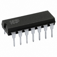
74HCT132N,652 NXP Semiconductors, 74HCT132N,652 Datasheet - Page 2

74HCT132N,652
Manufacturer Part Number
74HCT132N,652
Description
IC TRIGGER NAND QUAD 2IN 14DIP
Manufacturer
NXP Semiconductors
Series
74HCTr
Datasheets
1.74HCT4046ADB112.pdf
(19 pages)
2.74HCT4046ADB112.pdf
(23 pages)
3.74HC132N652.pdf
(8 pages)
Specifications of 74HCT132N,652
Number Of Circuits
4
Package / Case
14-DIP (0.300", 7.62mm)
Logic Type
NAND Gate - Schmitt Trigger
Number Of Inputs
2
Current - Output High, Low
5.2mA, 5.2mA
Voltage - Supply
4.5 V ~ 5.5 V
Operating Temperature
-40°C ~ 125°C
Mounting Type
Through Hole
Product
NAND
Logic Family
74HCT
High Level Output Current
- 4 mA
Low Level Output Current
4 mA
Propagation Delay Time
17 ns
Supply Voltage (max)
5.5 V
Supply Voltage (min)
4.5 V
Maximum Operating Temperature
+ 125 C
Mounting Style
SMD/SMT
Minimum Operating Temperature
- 40 C
Logical Function
NAND
Number Of Elements
4
Operating Supply Voltage (typ)
5V
Operating Temp Range
-40C to 125C
Package Type
PDIP
Number Of Outputs
1
Technology
CMOS
Mounting
Through Hole
Pin Count
14
Operating Temperature Classification
Automotive
Quiescent Current
2uA
Operating Supply Voltage (max)
5.5V
Operating Supply Voltage (min)
4.5V
Lead Free Status / RoHS Status
Lead free / RoHS Compliant
Lead Free Status / RoHS Status
Lead free / RoHS Compliant, Lead free / RoHS Compliant
Other names
568-1511-5
74HCT132N
933669150652
74HCT132N
933669150652
Philips Semiconductors
GENERAL
These family specifications cover the common electrical
ratings and characteristics of the entire HCMOS
74HC/HCT/HCU family, unless otherwise specified in the
individual device data sheet.
INTRODUCTION
The 74HC/HCT/HCU high-speed Si-gate CMOS logic
family combines the low power advantages of the
HE4000B family with the high speed and drive capability of
the low power Schottky TTL (LSTTL).
The family will have the same pin-out as the 74 series and
provide the same circuit functions.
In these families are included several HE4000B family
circuits which do not have TTL counterparts, and some
special circuits.
The basic family of buffered devices, designated as
XX74HCXXXXX, will operate at CMOS input logic levels
for high noise immunity, negligible typical quiescent supply
and input current. It is operated from a power supply of
2 to 6 V.
RECOMMENDED OPERATING CONDITIONS FOR 74HC/HCT
Note
1. For analog switches, e.g. “4016”, “4051 series”, “4351 series”, “4066” and “4067”, the specified maximum operating
March 1988
SYMBOL PARAMETER
V
V
V
T
T
t
r
, t
amb
amb
CC
I
O
HCMOS family characteristics
f
supply voltage is 10 V.
DC supply voltage
DC input voltage range
DC output voltage range
operating ambient temperature range
operating ambient temperature range
input rise and fall times except for
Schmitt-trigger inputs
min. typ. max. min. typ. max.
2.0
0
0
40
40
74HC
5.0
6.0
2
A subset of the family, designated as XX74HCTXXXXX,
with the same features and functions as the “HC-types”,
will operate at standard TTL power supply voltage
(5 V
pin-to-pin compatible CMOS replacements to reduce
power consumption without loss of speed. These types are
also suitable for converted switching from TTL to CMOS.
Another subset, the XX74HCUXXXXX, consists of
single-stage unbuffered CMOS compatible devices for
application in RC or crystal controlled oscillators and other
types of feedback circuits which operate in the linear
mode.
HANDLING MOS DEVICES
Inputs and outputs are protected against electrostatic
effects in a wide variety of device-handling situations.
However, to be totally safe, it is desirable to take handling
precautions into account
(see also “HANDLING PRECAUTIONS” ).
6.0
V
V
1000
500
400
85
125
CC
CC
10%) and logic input levels (0.8 to 2.0 V) for use as
4.5
0
0
40
40
74HCT
5.0
6.0
5.5
V
V
500
85
125
CC
CC
SPECIFICATIONS
UNIT CONDITIONS
V
V
V
ns
C
C
see DC and AC
CHAR. per device
V
V
V
CC
CC
CC
= 2.0 V
= 4.5 V
= 6.0 V
FAMILY


