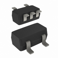
74LVC1G08GW/DG,125 NXP Semiconductors, 74LVC1G08GW/DG,125 Datasheet - Page 3

74LVC1G08GW/DG,125
Manufacturer Part Number
74LVC1G08GW/DG,125
Description
IC 2-INPUT AND GATE UMT5
Manufacturer
NXP Semiconductors
Series
74LVCr
Datasheet
1.74LVC1G08GW125.pdf
(17 pages)
Specifications of 74LVC1G08GW/DG,125
Number Of Circuits
1
Logic Type
AND Gate
Number Of Inputs
2
Current - Output High, Low
32mA, 32mA
Voltage - Supply
1.65 V ~ 5.5 V
Operating Temperature
-40°C ~ 125°C
Mounting Type
Surface Mount
Package / Case
SC-70-5, SC-88A, SOT-323-5, SOT-353, 5-TSSOP
Logic Family
74LVC
Supply Voltage (max)
5.5 V
Supply Voltage (min)
1.65 V
Maximum Operating Temperature
+ 125 C
Minimum Operating Temperature
- 40 C
Operating Temperature Range
- 40 C to + 125 C
Output Current
50 mA
Output Voltage
0 V to 5.5 V
Power Dissipation
250 mW
Lead Free Status / RoHS Status
Lead free / RoHS Compliant
Lead Free Status / RoHS Status
Lead free / RoHS Compliant, Lead free / RoHS Compliant
Other names
74LVC1G08GW/DG-G
74LVC1G08GW/DG-G
935283544125
74LVC1G08GW/DG-G
935283544125
NXP Semiconductors
6. Pinning information
Table 3.
7. Functional description
Table 4.
[1]
74LVC1G08
Product Specification
Symbol
B
A
GND
Y
n.c.
V
Input
A
L
L
H
H
Fig 4.
CC
H = HIGH voltage level; L = LOW voltage level
GND
B
A
Pin configuration
SOT353-1 and SOT753
Pin description
Function table
1
2
3
74LVC1G08
Pin
SOT353-1, SOT753
1
2
3
4
-
5
6.1 Pinning
6.2 Pin description
001aab638
[1]
5
4
V
Y
CC
SOT886, SOT891, SOT1115 and SOT1202
1
2
3
4
5
6
B
L
H
L
H
All information provided in this document is subject to legal disclaimers.
Fig 5.
Rev. 8 — 19 October 2010
GND
Pin configuration SOT886
B
A
Transparent top view
74LVC1G08
1
2
3
001aab639
6
5
4
V
n.c.
Y
CC
Output
Y
L
L
L
H
Fig 6.
Description
data input
data input
ground (0 V)
data output
not connected
supply voltage
GND
Pin configuration SOT891,
SOT1115 and SOT1202
B
A
Single 2-input AND gate
Transparent top view
74LVC1G08
74LVC1G08
1
2
3
© NXP B.V. 2010. All rights reserved.
001aae978
6
5
4
V
n.c.
Y
CC
3 of 17


