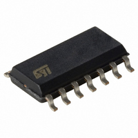
HCF4007UBM013TR STMicroelectronics, HCF4007UBM013TR Datasheet - Page 2

HCF4007UBM013TR
Manufacturer Part Number
HCF4007UBM013TR
Description
IC INVERTER DUAL COMPL 14-SOIC
Manufacturer
STMicroelectronics
Series
4000Br
Datasheet
1.HCF4007UBEY.pdf
(9 pages)
Specifications of HCF4007UBM013TR
Logic Type
Configurable Multiple Function
Number Of Circuits
2
Number Of Inputs
1
Schmitt Trigger Input
No
Output Type
Single-Ended
Current - Output High, Low
-6.8mA, 6.8mA
Voltage - Supply
3 V ~ 20 V
Operating Temperature
-55°C ~ 125°C
Mounting Type
Surface Mount
Package / Case
14-SOIC (3.9mm Width), 14-SOL
Logic Family
4000B
Number Of Channels Per Chip
3
Polarity
Inverting
Supply Voltage (max)
20 V
Supply Voltage (min)
3 V
Maximum Operating Temperature
+ 125 C
Mounting Style
SMD/SMT
High Level Output Current
- 2.4 mA
Low Level Output Current
2.4 mA
Maximum Power Dissipation
100 mW
Minimum Operating Temperature
- 55 C
Number Of Lines (input / Output)
3 / 3
Propagation Delay Time
110 ns at 5 V, 60 ns at 10 V, 50 ns at 15 V
Lead Free Status / RoHS Status
Lead free / RoHS Compliant
HCF4007UB
INPUT EQUIVALENT CIRCUIT
LOGIC DIAGRAM
ABSOLUTE MAXIMUM RATINGS
Absolute Maximum Ratings are those values beyond which damage to the device may occur. Functional operation under these conditions is
not implied.
All voltage values are referred to V
RECOMMENDED OPERATING CONDITIONS
2/9
Symbol
Symbol
V
V
T
T
T
P
V
V
stg
DD
I
DD
op
op
I
D
I
I
Supply Voltage
DC Input Voltage
DC Input Current
Power Dissipation per Package
Power Dissipation per Output Transistor
Operating Temperature
Storage Temperature
Supply Voltage
Input Voltage
Operating Temperature
SS
pin voltage.
Parameter
Parameter
PIN DESCRIPTION
6, 3, 10
PIN N°
13, 1
2, 11
8, 5
4, 9
12
14
7
SYMBOL
D
D
S
S
G
N1
N2
P2
P1
D
1
V
V
N/P3
to G
, S
, D
, D
, S
DD
SS
P3
N3
-0.5 to V
P2
N2
3
-55 to +125
-65 to +150
-0.5 to +22
-55 to 125
0 to V
3 to 20
Value
Value
Source Connections to
2nd and 3rd p-channel
transistors
Drain Connections from
the 1st and 2nd p-channel
transistors
Drain Connections from
the 1st and 2nd n-channel
transistors
Source Connections to
the 2nd and 3rd n-channel
Common connection to
the 3rd p-channel and
n-channel transistor
drains
Gate connections to
n-channel and p-channel
of the three transistor
pairs
Negative Supply Voltage
Positive Supply Voltage
200
100
NAME AND FUNCTION
10
DD
DD
+ 0.5
Unit
Unit
mW
mW
mA
°C
°C
°C
V
V
V
V


