HCF4042BEY STMicroelectronics, HCF4042BEY Datasheet
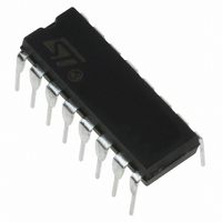
IC LATCH QUAD CLOCK D 16-DIP

HCF4042BEY

Manufacturer Part Number
HCF4042BEY
Description
IC LATCH QUAD CLOCK D 16-DIP
Manufacturer
STMicroelectronics
Series
4000Br
Datasheet

Specifications of HCF4042BEY

Logic Type
D-Type Transparent Latch
Circuit
4:4
Output Type
Differential
Voltage - Supply
3 V ~ 20 V
Independent Circuits
1
Delay Time - Propagation
40ns
Current - Output High, Low
6.8mA, 6.8mA
Operating Temperature
-55°C ~ 125°C
Mounting Type
Through Hole
Package / Case
16-DIP (0.300", 7.62mm)
Number Of Circuits
4
Logic Family
HCF40
Polarity
Inverting/Non-Inverting
High Level Output Current
- 2.4 mA
Low Level Output Current
32 mA
Propagation Delay Time
300 ns at 5 V, 150 ns at 10 V, 100 ns at 15 V
Supply Voltage (max)
20 V
Supply Voltage (min)
3 V
Maximum Operating Temperature
+ 125 C
Minimum Operating Temperature
- 55 C
Mounting Style
Through Hole
Lead Free Status / RoHS Status
Lead free / RoHS Compliant
Other names
497-1357-5

Available stocks

Company
Part Number
Manufacturer
Quantity
Price
Part Number:
HCF4042BEY
Quantity:
27
Part Number:
HCF4042BEY
Manufacturer:
STM
Quantity:
131 565
Part Number:
HCF4042BEY
Manufacturer:
ST
0
DESCRIPTION
The HCF4042B is a monolithic integrated circuit
fabricated
technology available in DIP and SOP packages.
The HCF4042B types contains four latch circuit,
each strobes by a common clock. Complementary
buffered outputs are available from each circuit.
The impedance of the n and p channel output
devices is balanced and all outputs are electrically
identical.
PIN CONNECTION
September 2001
CLOCK POLARITY CONTROL
Q AND Q OUTPUTS
COMMON CLOCK
LOW POWER TTL COMPATIBLE
STANDARDIZED SYMMETRICAL OUTPUT
CHARACTERISTICS
QUIESCENT CURRENT SPECIFIED UP TO
20V
5V, 10V AND 15V PARAMETRIC RATINGS
INPUT LEAKAGE CURRENT
I
100% TESTED FOR QUIESCENT CURRENT
MEETS ALL REQUIREMENTS OF JEDEC
JESD13B " STANDARD SPECIFICATIONS
FOR DESCRIPTION OF B SERIES CMOS
DEVICES"
I
= 100nA (MAX) AT V
in
Metal
Oxide
DD
= 18V T
Semiconductor
A
= 25°C
ORDER CODES
Information present at the data input is transferred
to outputs Q and Q during the CLOCK level which
is programmed by the POLARITY input. For
POLARITY = 0 the transfer occurs during the 0
CLOCK level and for POLARITY = 1 the transfer
occurs during the 1 CLOCK level. The outputs
follow the data input providing the CLOCK and
POLARITY levels defined above are present.
When a CLOCK transition occurs (positive for
POLARITY = 0 and negative for POLARITY = 1)
the information present at the input during the
CLOCK transition is retained at the outputs until
an opposite CLOCK transition occurs.
PACKAGE
QUAD CLOCKED D LATCH
SOP
DIP
DIP
HCF4042BM1
HCF4042BEY
TUBE
HCF4042B
HCF4042M013TR
SOP
T & R
1/9

Related parts for HCF4042BEY

HCF4042BEY Summary of contents

Page 1

... POLARITY levels defined above are present. When a CLOCK transition occurs (positive for POLARITY = 0 and negative for POLARITY = 1) the information present at the input during the CLOCK transition is retained at the outputs until an opposite CLOCK transition occurs. HCF4042B DIP SOP TUBE T & R HCF4042BEY HCF4042BM1 HCF4042M013TR 1/9 ...

Page 2

HCF4042B IINPUT EQUIVALENT CIRCUIT FUNCTIONAL DIAGRAM TRUTH TABLE CLOCK L H 2/9 PIN DESCRIPTION PIN No SYMBOL 10 CLOCK ...

Page 3

LOGIC BLOCK DIAGRAM This logic diagram has not be used to estimate propagation delays ABSOLUTE MAXIMUM RATINGS Symbol V Supply Voltage Input Voltage Input Current I P Power Dissipation per Package D Power Dissipation ...

Page 4

HCF4042B DC SPECIFICATIONS Symbol Parameter V (V) I Quiescent Current 0/5 L 0/10 0/15 0/20 V High Level Output 0/5 OH Voltage 0/10 0/15 V Low Level Output 5/0 OL Voltage 10/0 15/0 V High Level Input IH Voltage V ...

Page 5

DYNAMIC ELECTRICAL CHARACTERISTICS (T Symbol Parameter t t Propagation Delay Time PLH PHL (DATA Propagation Delay Time PLH PHL (DATA Propagation Delay Time PLH PHL (CLOCK ...

Page 6

HCF4042B TEST CIRCUIT C = 50pF or equivalent (includes jig and probe capacitance 200K pulse generator (typically OUT 6/9 ...

Page 7

Plastic DIP-16 (0.25) MECHANICAL DATA mm. DIM. MIN. a1 0. 17. TYP MAX. MIN. 0.020 1.65 0.030 0.5 0.25 20 8.5 2.54 7.1 5.1 3.3 1.27 HCF4042B inch ...

Page 8

HCF4042B DIM. MIN 0 0. 9 3.8 G 4 8/9 SO-16 MECHANICAL DATA mm. TYP MAX. 1.75 0.2 1.65 0.46 0.25 0.5 ...

Page 9

... No license is granted by implication or otherwise under any patent or patent rights of STMicroelectronics. Specifications mentioned in this publication are subject to change without notice. This publication supersedes and replaces all information previously supplied ...

Related keywords