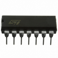
HCF4047BEY STMicroelectronics, HCF4047BEY Datasheet - Page 9

HCF4047BEY
Manufacturer Part Number
HCF4047BEY
Description
IC MULTIVIBRATOR LOW PWR 14-DIP
Manufacturer
STMicroelectronics
Series
4000Br
Specifications of HCF4047BEY
Logic Type
Astable, Monostable
Independent Circuits
1
Schmitt Trigger Input
No
Propagation Delay
125ns
Current - Output High, Low
6.8mA, 6.8mA
Voltage - Supply
3 V ~ 20 V
Operating Temperature
-55°C ~ 125°C
Mounting Type
Through Hole
Package / Case
14-DIP (0.300", 7.62mm)
Elements Per Chip
1
Logic Family
4000B
Input Bias Current (max)
0.02 mA
Propagation Delay Time
1000 ns, 450 ns, 300 ns
High Level Output Current
- 2.4 mA
Low Level Output Current
2.4 mA
Supply Voltage (max)
20 V
Supply Voltage (min)
3 V
Maximum Operating Temperature
+ 125 C
Minimum Operating Temperature
- 55 C
Mounting Style
Through Hole
Operating Supply Voltage
3.3 V, 5 V, 9 V, 12 V
Capacitance, Input
5 pF (Typ.)
Circuit Type
Monolithic Integrated
Current, Input
±10 mA
Current, Input, Leakage
± 1 μA (Max.)
Current, Supply
600 μA
Logic Function
Multivibrator
Number Of Circuits
Triple
Package Type
DIP-14
Power Dissipation
200 mW (Per Package)
Special Features
Astable/Monostable
Temperature, Operating, Maximum
125 °C
Temperature, Operating, Minimum
-55 °C
Temperature, Operating, Range
-55 to +125 °C
Time, Delay, Propagation
200 to 80 ns (Typ.)
Voltage, Supply
3 to 20 V
Lead Free Status / RoHS Status
Contains lead / RoHS non-compliant
Other names
497-1358-5
Available stocks
Company
Part Number
Manufacturer
Quantity
Price
Company:
Part Number:
HCF4047BEY
Manufacturer:
AVAGO
Quantity:
5 000
6 - POWER CONSUMPTION
In the standby mode (Monostable or Astable),
power dissipation will be a function of leakage
current in the circuit, as shown in the static
electrical characteristics. For dynamic operation,
the power needed to charge the external timing
capacitor C is given by the following formula :
Astable Mode :
P = 2CV
P = 4CV
Monostable Mode : P = ——————————
(Output at Pin 10 and 11)
The circuit is designed so that most of the total
power is consumed in the external components. In
practice, the lower the values of frequency and
voltage used, the closer the actual power
dissipation will be to the calculated value.
Because the power dissipation does not depend
on R, a design for minimum power dissipation
would be a small value of C. The value of R would
depend on the desired period (within the
limitations discussed above).
7 - TIMING-COMPONENT LIMITATIONS
TEST CIRCUIT
C
R
R
L
L
T
= 50pF or equivalent (includes jig and probe capacitance)
= 200K
= Z
OUT
of pulse generator (typically 50 )
2
2
f. (Output at Pin 13)
f. (Output at Pin 10 and 11)
(2.9CV
2
) (Duty Cycle)
T
The capacitor used in the circuit should be
non-polarized and have low leakage (i.e. the
parallel resistance of the capacitor should be an
order of magnitude greater than the external
resistor used). Three is no upper or lower limit for
either R or C value to maintain oscillation.
However, in consideration of accuracy, C must be
much larger than the inherent stray capacitance in
the system (unless this capacitance can be
measured and taken into account). R must be
much larger than the COS/MOS "ON" resistance
in series with it, which typically is hundreds of
ohms. In addition, with very large values of R,
some short-term instability with respect to time
may be noted.
The recommended values for these components
to maintain agreement with previously calculated
formulas without trimming should be :
C > 100pF, up to any practical value, for astable
modes ;
C > 1000pF, up to any practical value, for
monostable modes.
10K < R < 1M .
HCF4047B
9/12


