HCF4094BEY STMicroelectronics, HCF4094BEY Datasheet
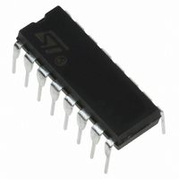
IC BUS REGISTER 8STAGE 16-DIP

HCF4094BEY

Manufacturer Part Number
HCF4094BEY
Description
IC BUS REGISTER 8STAGE 16-DIP
Manufacturer
STMicroelectronics
Series
4000Br
Datasheet

Specifications of HCF4094BEY

Logic Type
Shift Register
Output Type
Standard
Number Of Elements
1
Number Of Bits Per Element
8
Function
Serial to Parallel
Voltage - Supply
3 V ~ 20 V
Operating Temperature
-55°C ~ 125°C
Mounting Type
Through Hole
Package / Case
16-DIP (0.300", 7.62mm)
Counting Sequence
Serial to Serial/Parallel
Number Of Circuits
1
Logic Family
HCF40
Propagation Delay Time
600 ns, 250 ns, 190 ns
Supply Voltage (max)
20 V
Maximum Operating Temperature
+ 125 C
Minimum Operating Temperature
- 55 C
Mounting Style
Through Hole
Operating Supply Voltage
3 V to 20 V
Lead Free Status / RoHS Status
Lead free / RoHS Compliant
Other names
497-1373-5

Available stocks

Company
Part Number
Manufacturer
Quantity
Price
Part Number:
HCF4094BEY
Quantity:
10
Part Number:
HCF4094BEY
Manufacturer:
ST
0
Part Number:
HCF4094BEY
Manufacturer:
ST
Quantity:
20 000
Part Number:
HCF4094BEY(ROHS)
Manufacturer:
ST
0
Part Number:
HCF4094BEY,HCF4094BE
Manufacturer:
ST
0
DESCRIPTION
The HCF4094B is a monolithic integrated circuit
fabricated
technology available in DIP and SOP packages.
The HCF4094B is an 8 stages serial shift register
having a storage latch associated with each stage
for strobing data from the serial input to parallel
buffered 3-state outputs. The parallel outputs may
be connected directly to common bus lines. Data
is shifted on positive clock transition. The data in
each shift register stage is transferred to the
PIN CONNECTION
March 2004
3-STATE PARALLEL OUTPUTS FOR
CONNECTION TO COMMON BUS
SEPARATE SERIAL OUTPUTS
SYNCHRONOUS TO BOTH POSITIVE AND
NEGATIVE CLOCK EDGES FOR
CASCADING
MEDIUM SPEED OPERATION 5MHz at 10V
QUIESCENT CURRENT SPECIFIED UP TO
20V
STANDARDIZED SYMMETRICAL OUTPUT
CHARACTERISTICS
5V, 10V AND 15V PARAMETRIC RATINGS
INPUT LEAKAGE CURRENT
I
100% TESTED FOR QUIESCENT CURRENT
I
= 100nA (MAX) AT V
in
Metal
Oxide
DD
8 STAGE SHIFT AND STORE BUS REGISTER
= 18V T
Semiconductor
A
= 25°C
ORDER CODES
storage register when the STROBE input is high.
Data in the storage register appears at the outputs
whenever the OUTPUT-ENABLE signal is high.
Two serial outputs are available for cascading a
number of HCF4094B devices. Data is available
at the Q
edges to allow for high speed operation in
cascaded system in which the clock rise time is
fast. The same serial information, available at the
Q’
provides a means for cascading HCF4094B
devices when the clock rise time is slow.
PACKAGE
S
SOP
DIP
terminal on the next negative clock edge,
WITH 3-STATE OUTPUTS
S
serial output terminal on positive clock
DIP
HCF4094BM1
HCF4094BEY
TUBE
HCF4094B
HCF4094M013TR
SOP
T & R
1/13

Related parts for HCF4094BEY

HCF4094BEY Summary of contents

Page 1

... The same serial information, available at the Q’ terminal on the next negative clock edge, S provides a means for cascading HCF4094B devices when the clock rise time is slow. HCF4094B DIP SOP TUBE T & R HCF4094BEY HCF4094BM1 HCF4094M013TR serial output terminal on positive clock 1/13 ...

Page 2

HCF4094B IINPUT EQUIVALENT CIRCUIT FUNCTIONAL DIAGRAM TRUTH TABLE OUTPUTS CLOCK STROBE ENABLE Don’t Care OC : Open Circuit * At the positive clock edge information on the 7th shift register stage is ...

Page 3

LOGIC DIAGRAM TIMING CHART HCF4094B 3/13 ...

Page 4

HCF4094B ABSOLUTE MAXIMUM RATINGS Symbol V Supply Voltage Input Voltage Input Current I P Power Dissipation per Package D Power Dissipation per Output Transistor T Operating Temperature op T Storage Temperature stg Absolute Maximum ...

Page 5

DC SPECIFICATIONS Symbol Parameter V (V) I Quiescent Current 0/5 L 0/10 0/15 0/20 V High Level Output 0/5 OH Voltage 0/10 0/15 V Low Level Output 5/0 OL Voltage 10/0 15/0 V High Level Input IH Voltage V Low ...

Page 6

HCF4094B DYNAMIC ELECTRICAL CHARACTERISTICS (T Symbol Parameter t t Propagation Delay Time PLH PHL (Clock to serial Output Propagation Delay Time PLH PHL (Clock to serial Output Q’ Propagation Delay Time PLH PHL (Clock to ...

Page 7

TYPICAL APPLICATION (REMOTE CONTROL HOLDING REGISTER) TEST CIRCUIT PLH PHL PZL PLZ PZH PHZ C = 50pF or equivalent (includes jig and probe capacitance 200K ...

Page 8

HCF4094B WAVEFORM 1: PROPAGATION DELAY TIMES, PULSE WIDTH (CLOCK), SETUP AND HOLD TIME (DATA IN TO CLOCK) (f=1MHz; 50% duty cycle) WAVEFORM 2: PROPAGATION DELAY TIME, PULSE WIDTH (STROBE), SETUP AND HOLD TIME (STROBE TO CLOCK) (f=1MHz; 50% duty cycle) ...

Page 9

WAVEFORM 3: OUTPUT ENABLE AND DISABLE TIME (f=1MHz; 50% duty cycle) HCF4094B 9/13 ...

Page 10

HCF4094B DIM. MIN. a1 0. 10/13 Plastic DIP-16 (0.25) MECHANICAL DATA mm. TYP MAX. 1.65 0.5 0.25 20 8.5 2.54 17.78 7.1 5.1 3.3 1.27 inch MIN. TYP. ...

Page 11

SO-16 MECHANICAL DATA mm. DIM. MIN 0 0. 9 3.8 G 4 TYP MAX. MIN. 1.75 0.2 0.004 1.65 0.46 0.013 ...

Page 12

HCF4094B DIM. MIN 12 6.45 Bo 10.3 Ko 2.1 Po 3.9 P 7.9 12/13 Tape & Reel SO-16 MECHANICAL DATA mm. TYP MAX. 330 13.2 22.4 6.65 10.5 2.3 4.1 8.1 inch ...

Page 13

... No license is granted by implication or otherwise under any patent or patent rights of STMicroelectronics. Specifications mentioned in this publication are subject to change without notice. This publication supersedes and replaces all information previously supplied ...

Related keywords