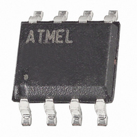
AT24C1024BN-SH25-B Atmel, AT24C1024BN-SH25-B Datasheet - Page 5

AT24C1024BN-SH25-B
Manufacturer Part Number
AT24C1024BN-SH25-B
Description
IC EEPROM 1MBIT 1MHZ 8SOIC
Manufacturer
Atmel
Datasheet
1.AT24C1024BN-SH25-B.pdf
(25 pages)
Specifications of AT24C1024BN-SH25-B
Format - Memory
EEPROMs - Serial
Memory Type
EEPROM
Memory Size
1M (128K x 8)
Speed
1MHz
Interface
I²C, 2-Wire Serial
Voltage - Supply
2.5 V ~ 5.5 V
Operating Temperature
-40°C ~ 85°C
Package / Case
8-SOIC (3.9mm Width)
Organization
128 K x 8
Interface Type
2-Wire
Maximum Clock Frequency
1 MHz
Access Time
550 ns
Supply Voltage (max)
5.5 V
Supply Voltage (min)
1.8 V
Maximum Operating Current
3 mA
Maximum Operating Temperature
+ 85 C
Mounting Style
SMD/SMT
Minimum Operating Temperature
- 40 C
Operating Supply Voltage
3.3 V, 5 V
Memory Configuration
131072 X 8
Clock Frequency
1MHz
Supply Voltage Range
2.5V To 5.5V
Memory Case Style
SOIC
No. Of Pins
8
Rohs Compliant
Yes
Density
1Mb
Access Time (max)
550ns
Frequency (max)
1MHz
Write Protection
Yes
Data Retention
40Year
Operating Supply Voltage (typ)
3.3/5V
Operating Temp Range
-40C to 85C
Supply Current
3mA
Operating Supply Voltage (min)
2.5V
Operating Supply Voltage (max)
5.5V
Operating Temperature Classification
Industrial
Mounting
Surface Mount
Pin Count
8
Lead Free Status / RoHS Status
Lead free / RoHS Compliant
Available stocks
Company
Part Number
Manufacturer
Quantity
Price
Company:
Part Number:
AT24C1024BN-SH25-B
Manufacturer:
AMTLE
Quantity:
1 760
Part Number:
AT24C1024BN-SH25-B
Manufacturer:
MICROCHIP/微芯
Quantity:
20 000
Table 3-3.
Applicable over recommended operating range from T
erwise noted). Test conditions are listed in Note 2.
Notes:
4. Device Operation
5194F–SEEPR–1/08
Symbol
t
t
t
t
t
t
t
t
t
t
t
t
Endurance
i
AA
BUF
HD.STA
SU.STA
HD.DAT
SU.DAT
R
F
SU.STO
DH
WR
1. This parameter is ensured by characterization only.
2. AC measurement conditions:
(1)
R
Input pulse voltages: 0.3 V
Input rise and fall times: ≤ 50 ns
Input and output timing reference voltages: 0.5 V
AC Characteristics (Industrial Temperature)
L
(connects to V
Parameter
Noise Suppression Time
Clock Low to Data Out Valid
Time the bus must be free before a
new transmission can start
Start Hold Time
Start Set-up Time
Data In Hold Time
Data In Set-up Time
Inputs Rise Time
Inputs Fall Time
Stop Set-up Time
Data Out Hold Time
Write Cycle Time
25°C, Page Mode, 3.3V
CLOCK and DATA TRANSITIONS: The SDA pin is normally pulled high with an external
device. Data on the SDA pin may change only during SCL low time periods (see
page
below.
CC
(1)
): 1.3 kΩ (2.5V, 5V), 10 kΩ (1.8V)
7). Data changes during SCL high periods will indicate a start or stop condition as defined
(1)
CC
(1)
to 0.7 V
(1)
CC
AI
0.05
Min
100
1.3
0.6
0.6
0.6
50
0
= −40°C to +85°C, V
CC
1.8-volt
Max
100
300
0.9
0.3
5
1,000,000
0.05
0.25
0.25
0.25
Min
100
0.5
50
0
CC
2.5, 5.0-volt
= +1.8V to +3.6V, CL = 100 pF (unless oth-
Max
0.55
100
0.3
50
5
Cycles
Units
Write
ms
µs
µs
µs
µs
µs
ns
µs
µs
ns
ns
ns
Figure 4-4 on
5


