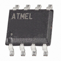
AT24C1024BN-SH25-B Atmel, AT24C1024BN-SH25-B Datasheet - Page 8

AT24C1024BN-SH25-B
Manufacturer Part Number
AT24C1024BN-SH25-B
Description
IC EEPROM 1MBIT 1MHZ 8SOIC
Manufacturer
Atmel
Datasheet
1.AT24C1024BN-SH25-B.pdf
(25 pages)
Specifications of AT24C1024BN-SH25-B
Format - Memory
EEPROMs - Serial
Memory Type
EEPROM
Memory Size
1M (128K x 8)
Speed
1MHz
Interface
I²C, 2-Wire Serial
Voltage - Supply
2.5 V ~ 5.5 V
Operating Temperature
-40°C ~ 85°C
Package / Case
8-SOIC (3.9mm Width)
Organization
128 K x 8
Interface Type
2-Wire
Maximum Clock Frequency
1 MHz
Access Time
550 ns
Supply Voltage (max)
5.5 V
Supply Voltage (min)
1.8 V
Maximum Operating Current
3 mA
Maximum Operating Temperature
+ 85 C
Mounting Style
SMD/SMT
Minimum Operating Temperature
- 40 C
Operating Supply Voltage
3.3 V, 5 V
Memory Configuration
131072 X 8
Clock Frequency
1MHz
Supply Voltage Range
2.5V To 5.5V
Memory Case Style
SOIC
No. Of Pins
8
Rohs Compliant
Yes
Density
1Mb
Access Time (max)
550ns
Frequency (max)
1MHz
Write Protection
Yes
Data Retention
40Year
Operating Supply Voltage (typ)
3.3/5V
Operating Temp Range
-40C to 85C
Supply Current
3mA
Operating Supply Voltage (min)
2.5V
Operating Supply Voltage (max)
5.5V
Operating Temperature Classification
Industrial
Mounting
Surface Mount
Pin Count
8
Lead Free Status / RoHS Status
Lead free / RoHS Compliant
Available stocks
Company
Part Number
Manufacturer
Quantity
Price
Company:
Part Number:
AT24C1024BN-SH25-B
Manufacturer:
AMTLE
Quantity:
1 760
Part Number:
AT24C1024BN-SH25-B
Manufacturer:
MICROCHIP/微芯
Quantity:
20 000
Figure 4-5.
Figure 4-6.
5. Device Addressing
8
AT24C1024B
Start and Stop Definition
Output Acknowledge
DATA OUT
DATA IN
The 1024K EEPROM requires an 8-bit device address word following a start condition to enable
the chip for a read or write operation (see
sists of a mandatory one, zero sequence for the first four most significant bits as shown. This is
common to all two-wire EEPROM devices.
The 1024K uses the two device address bit, A1, A2, to allow up to four devices on the same bus.
These A1, A2 bits must compare to the corresponding hardwired input pins. The A1, A2 pin uses
an internal proprietary circuit that biases it to a logic low condition if the pin is allowed to float.
The seventh bit (P
address bit is the most significant bit of the data word address that follows. The eighth bit of the
device address is the read/write operation select bit. A read operation is initiated if this bit is high
and a write operation is initiated if this bit is low.
Upon a compare of the device address, the EEPROM will output a zero. If a compare is not
made, the device will return to a standby state.
SDA
SCL
SCL
START
START
0
) of the device address is a memory page address bit. This memory page
1
Figure 7-1 on page
8
ACKNOWLEDGE
STOP
9
11). The device address word con-
5194F–SEEPR–1/08


