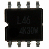
BR93L46F-WE2 Rohm Semiconductor, BR93L46F-WE2 Datasheet - Page 12

BR93L46F-WE2
Manufacturer Part Number
BR93L46F-WE2
Description
IC EEPROM 1KBIT 2MHZ 8SOP
Manufacturer
Rohm Semiconductor
Specifications of BR93L46F-WE2
Memory Size
1K (64 x 16)
Format - Memory
EEPROMs - Serial
Memory Type
EEPROM
Speed
2MHz
Interface
Microwire, 3-Wire Serial
Voltage - Supply
1.8 V ~ 5.5 V
Operating Temperature
-40°C ~ 85°C
Package / Case
8-SOP
Clock Frequency
2MHz
Supply Voltage Range
1.8V To 5.5V
Memory Case Style
SOP
No. Of Pins
8
Operating Temperature Range
-40°C To +85°C
Svhc
No SVHC (18-Jun-2010)
Package /
RoHS Compliant
Organization
64 K x 16
Interface Type
Microwire
Maximum Clock Frequency
2 MHz
Supply Voltage (max)
5.5 V
Supply Voltage (min)
1.8 V
Maximum Operating Temperature
+ 85 C
Mounting Style
SMD/SMT
Minimum Operating Temperature
- 40 C
Operating Supply Voltage
1.8 V, 5.5 V
Memory Configuration
64 X 16
Rohs Compliant
Yes
Lead Free Status / RoHS Status
Lead free / RoHS Compliant
Lead Free Status / RoHS Status
Lead free / RoHS Compliant
Other names
BR93L46F-WE2TR
Available stocks
Company
Part Number
Manufacturer
Quantity
Price
Part Number:
BR93L46F-WE2
Manufacturer:
ROHM/罗姆
Quantity:
20 000
●Timing chart
© 2011 ROHM Co., Ltd. All rights reserved.
BR93L□□-W Series, 93A□□-WM Series, BR93H□□-WC Series
www.rohm.com
1) Read cycle (READ)
*1 Start bit
○When the read command is recognized, input address data (16bit) is output to serial. And at that moment, at taking A0, in
○In this command, input 16bit data (D15~D0) are written to designated addresses (Am~A0). The actual write starts by the fall
○In this command, input 16bit data is written simultaneously to all adresses. Data is not written continuously per one word
2) Write cycle (WRITE)
3) Write all cycyle (WRAL)
sync with the rise of SK, “0” (dummy bit) is output. And, the following data is output in sync with the rise of SK.
This IC has an address auto increment function valid only at read command. This is the function where after the above read
execution, by continuously inputting SK clock, the above address data is read sequentially. And, during the auto increment,
keep CS at “H”.
but is written in bulk, the write time is only Max. 5ms in conformity with tE/W.
of CS of D0 taken SK clock.
When STATUS is not detected, (CS=”L” fixed) Max. 5ms in conformity with tE/W, and when STATUS is detected (CS=”H”),
all commands are not accepted for areas where “L” (BUSY) is output from D0, therefore, do not input any command.
When data “1” is input for the first time after the rise of CS, this is recognized as a start bit. And when “1” is input after plural “0” are input, it is recognized as a
start bit, and the following operation is started. This is common to all the commands to described hereafter.
CS
SK
DI
DO
CS
SK
DI
DO
CS
SK
DI
DO
High-Z
High-Z
High-Z
1
*1
1
1
1
1
1
1
2
0
2
0
2
0
1
0
Am
4
Am
0
4
1
5
~ ~
~ ~
~ ~
~ ~
~ ~
~ ~
~ ~
~ ~
~ ~
~ ~
~ ~
~ ~
~ ~
~ ~
A1
A1
Fig.62 Write all cycle
Fig. 60 Read cycle
Fig.61 Write cycle
A0
A0
0
D15 D14
D15 D14
D15 D14
12/40
~ ~
~ ~
~ ~
~ ~
~ ~
~ ~
~ ~
~ ~
~ ~
~ ~
~ ~
~ ~
~ ~
D1
D1
D1
n
D0
D0
tCS
D0
n
tCS
n
n+1
D15 D14
*2
tE/W
tE/W
BUSY
BUSY
tSV
~ ~
~ ~
~ ~
~ ~
tSV
~ ~
STATUS
~ ~
~ ~
~ ~
~ ~
~ ~
STATUS
READY
READY
~ ~
~ ~
~ ~
~ ~
BR93L46-W/A46-WM : n=25, m=5
BR93L56-W/A56-WM
BR93L66-W/A66-WM
BR93L76-W/A76-WM
BR93L86-W/A86-WM
BR93L46-W/A46-WM : n=25
BR93L56-W/A56-WM
BR93L66-W/A66-WM
BR93L76-W/A76-WM
BR93L86-W/A86-WM
BR93L46-W/A46-WM : n=25, m=5
BR93L56-W/A56-WM
BR93L66-W/A66-WM
BR93L76-W/A76-WM
BR93L86-W/A86-WM
Technical Note
2011.02 - Rev.F
: n=27, m=7
: n=29, m=9
: n=27
: n=29
: n=27, m=7
: n=29, m=9


