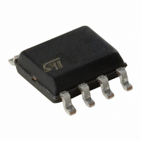
M93S46-WMN6TP STMicroelectronics, M93S46-WMN6TP Datasheet - Page 15

M93S46-WMN6TP
Manufacturer Part Number
M93S46-WMN6TP
Description
IC EEPROM 1KBIT 2MHZ 8SOIC
Manufacturer
STMicroelectronics
Datasheet
1.M93S46-WMN6TP.pdf
(34 pages)
Specifications of M93S46-WMN6TP
Format - Memory
EEPROMs - Serial
Memory Type
EEPROM
Memory Size
1K (64 x 16)
Speed
2MHz
Interface
Microwire, 3-Wire Serial
Voltage - Supply
2.5 V ~ 5.5 V
Operating Temperature
-40°C ~ 85°C
Package / Case
8-SOIC (3.9mm Width)
Organization
64 K x 16
Interface Type
Microwire
Maximum Clock Frequency
2 MHz
Supply Voltage (max)
5.5 V
Supply Voltage (min)
2.5 V
Maximum Operating Current
2 mA
Maximum Operating Temperature
+ 85 C
Mounting Style
SMD/SMT
Minimum Operating Temperature
- 40 C
Operating Supply Voltage
3.3 V, 5 V
Density
1Kb
Frequency (max)
2MHz
Write Protection
Yes
Data Retention
40Year
Operating Supply Voltage (typ)
3.3/5V
Package Type
SOIC N
Operating Temp Range
-40C to 85C
Supply Current
2mA
Operating Supply Voltage (min)
2.5V
Operating Supply Voltage (max)
5.5V
Operating Temperature Classification
Industrial
Mounting
Surface Mount
Pin Count
8
Lead Free Status / RoHS Status
Lead free / RoHS Compliant
Other names
497-8666-2
M93S46-WMN6TP
M93S46-WMN6TP
Available stocks
Company
Part Number
Manufacturer
Quantity
Price
Part Number:
M93S46-WMN6TP
Manufacturer:
ST
Quantity:
20 000
ing the Protection Register Write (PRWRITE) in-
struction. When the OTP bit is set, the Ready/Busy
status cannot appear on Serial Data Output (Q).
When the OTP bit is not set, the Busy status ap-
pears on Serial Data Output (Q).
Note: A Protection Register Enable (PREN) in-
struction must immediately precede the Protection
Register Disable (PRDS) instruction.
Figure 8. Write Sequence with One Clock Glitch
CLOCK PULSE COUNTER
In a noisy environment, the number of pulses re-
ceived on Serial Clock (C) may be greater than the
number delivered by the Bus Master (the micro-
controller). This can lead to a misalignment of the
instruction of one or more bits (as shown in
8.) and may lead to the writing of erroneous data
at an erroneous address.
To combat this problem, the M93Sx6 has an on-
chip counter that counts the clock pulses from the
start bit until the falling edge of the Chip Select In-
put (S). If the number of clock pulses received is
not the number expected, the WRITE, PAWRITE,
WRALL, PRWRITE or PRCLEAR instruction is
S
D
C
START
"0"
WRITE
"1"
Figure
An
Glitch
An-1
COMMON I/O OPERATION
Serial Data Output (Q) and Serial Data Input (D)
can be connected together, through a current lim-
iting resistor, to form a common, single-wire data
bus. Some precautions must be taken when oper-
ating the memory in this way, mostly to prevent a
short circuit current from flowing when the last ad-
dress bit (A0) clashes with the first data bit on Se-
rial Data Output (Q). Please see the application
note AN394 for details.
aborted, and the contents of the memory are not
modified.
The number of clock cycles expected for each in-
struction, and for each member of the M93Sx6
family, are summarized in
example, a Write Data to Memory (WRITE) in-
struction on the M93S56 (or M93S66) expects 27
clock cycles from the start bit to the falling edge of
Chip Select Input (S). That is:
ARE SHIFTED BY ONE BIT
ADDRESS AND DATA
An-2
1 Start bit
+ 2 Op-code bits
+ 8 Address bits
+ 16 Data bits
M93S66, M93S56, M93S46
D0
Table 2.
to
AI01395
Table
3.. For
15/34


