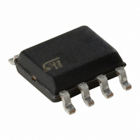
M93C66-WMN6P STMicroelectronics, M93C66-WMN6P Datasheet - Page 10

M93C66-WMN6P
Manufacturer Part Number
M93C66-WMN6P
Description
IC EEPROM 4KBIT 2MHZ 8SOIC
Manufacturer
STMicroelectronics
Datasheets
1.M93C46-WMN6TP.pdf
(36 pages)
2.M93C46-WMN6TP.pdf
(37 pages)
3.M93C46-WBN6P.pdf
(31 pages)
Specifications of M93C66-WMN6P
Format - Memory
EEPROMs - Serial
Memory Type
EEPROM
Memory Size
4K (512 x 8 or 256 x 16)
Speed
2MHz
Interface
Microwire, 3-Wire Serial
Voltage - Supply
2.5 V ~ 5.5 V
Operating Temperature
-40°C ~ 85°C
Package / Case
8-SOIC (3.9mm Width)
Organization
512 x 8
Interface Type
Microwire
Maximum Clock Frequency
2 MHz
Supply Voltage (max)
5.5 V
Supply Voltage (min)
2.5 V
Maximum Operating Current
2 mA
Maximum Operating Temperature
+ 85 C
Mounting Style
SMD/SMT
Minimum Operating Temperature
- 40 C
Operating Supply Voltage
2.5 V, 5.5 V
Memory Configuration
512 X 8, 256 X 16
Clock Frequency
2MHz
Supply Voltage Range
2.5V To 5.5V
Memory Case Style
SOIC
No. Of Pins
8
Rohs Compliant
Yes
Lead Free Status / RoHS Status
Lead free / RoHS Compliant
Other names
497-5672-5
Available stocks
Company
Part Number
Manufacturer
Quantity
Price
Part Number:
M93C66-WMN6P
Manufacturer:
ST
Quantity:
20 000
M93C86, M93C76, M93C66, M93C56, M93C46
Erase All
The Erase All Memory (ERAL) instruction erases
the whole memory (all memory bits are set to 1).
The format of the instruction requires that a dum-
my address be provided. The Erase cycle is con-
ducted in the same way as the Erase instruction
(ERASE). The completion of the cycle can be de-
tected by monitoring the Ready/Busy line, as de-
scribed in the
Figure 6. WRAL Sequence
Note: For the meanings of Xn and Dn, please see
10/31
WRITE
ALL
READY/BUSY STATUS
S
Q
D
1
CODE
0
OP
0 0
1 Xn X0
ADDR
Table
section.
5.,
Dn
Table 6.
and
DATA IN
Write All
As with the Erase All Memory (ERAL) instruction,
the format of the Write All Memory with same Data
(WRAL) instruction requires that a dummy ad-
dress be provided. As with the Write Data to Mem-
ory (WRITE) instruction, the format of the Write All
Memory with same Data (WRAL) instruction re-
quires that an 8-bit data byte, or 16-bit data word,
be provided. This value is written to all the ad-
dresses of the memory device. The completion of
the cycle can be detected by monitoring the
Ready/Busy line, as described next.
Table
7..
D0
BUSY
STATUS
CHECK
READY
AI00880C


