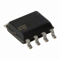
M93C66-WMN6P STMicroelectronics, M93C66-WMN6P Datasheet - Page 19

M93C66-WMN6P
Manufacturer Part Number
M93C66-WMN6P
Description
IC EEPROM 4KBIT 2MHZ 8SOIC
Manufacturer
STMicroelectronics
Datasheets
1.M93C46-WMN6TP.pdf
(36 pages)
2.M93C46-WMN6TP.pdf
(37 pages)
3.M93C46-WBN6P.pdf
(31 pages)
Specifications of M93C66-WMN6P
Format - Memory
EEPROMs - Serial
Memory Type
EEPROM
Memory Size
4K (512 x 8 or 256 x 16)
Speed
2MHz
Interface
Microwire, 3-Wire Serial
Voltage - Supply
2.5 V ~ 5.5 V
Operating Temperature
-40°C ~ 85°C
Package / Case
8-SOIC (3.9mm Width)
Organization
512 x 8
Interface Type
Microwire
Maximum Clock Frequency
2 MHz
Supply Voltage (max)
5.5 V
Supply Voltage (min)
2.5 V
Maximum Operating Current
2 mA
Maximum Operating Temperature
+ 85 C
Mounting Style
SMD/SMT
Minimum Operating Temperature
- 40 C
Operating Supply Voltage
2.5 V, 5.5 V
Memory Configuration
512 X 8, 256 X 16
Clock Frequency
2MHz
Supply Voltage Range
2.5V To 5.5V
Memory Case Style
SOIC
No. Of Pins
8
Rohs Compliant
Yes
Lead Free Status / RoHS Status
Lead free / RoHS Compliant
Other names
497-5672-5
Available stocks
Company
Part Number
Manufacturer
Quantity
Price
Part Number:
M93C66-WMN6P
Manufacturer:
ST
Quantity:
20 000
Table 21. AC Characteristics (M93Cx6-W, Device Grade 6)
Note: 1. t
Symbol
t
t
t
t
t
t
t
t
t
t
t
t
SLSH
CHCL
CLCH
t
CHQV
SHCH
DVCH
CHDX
SHQV
CHQL
SLCH
CLSH
SLQZ
CLSL
t
f
W
C
2. Chip Select Input (S) must be brought Low for a minimum of tSLSH between consecutive instruction cycles.
3. Current product: identified by Process Identification letter F or M.
4. New product: identified by Process Identification letter W or G or S.
2
1
1
CHCL
+ t
t
t
t
t
t
t
t
Alt.
t
t
t
CSS
t
SKH
CSH
f
SKS
t
t
PD0
PD1
SKL
DIH
DIS
WP
CLCH
SK
CS
SV
DF
1 / f
Clock Frequency
Chip Select Low to Clock High
Chip Select Set-up Time
Chip Select Low to Chip Select High
Clock High Time
Clock Low Time
Data In Set-up Time
Data In Hold Time
Clock Set-up Time (relative to S)
Chip Select Hold Time
Chip Select to Ready/Busy Status
Chip Select Low to Output Hi-Z
Delay to Output Low
Delay to Output Valid
Erase/Write Cycle time
C
.
Test conditions specified in
Parameter
M93C86, M93C76, M93C66, M93C56, M93C46
Table 13.
Min.
1000
D.C.
250
100
350
250
100
100
100
0
3
and
Max.
Table 10.
400
400
400
200
10
1
3
Min.
D.C.
200
200
200
50
50
50
50
50
0
4
Max.
200
100
200
200
2
5
4
MHz
Unit
ms
ns
ns
ns
ns
ns
ns
ns
ns
ns
ns
ns
ns
ns
19/31


