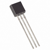
DS2502-E48+ Maxim Integrated Products, DS2502-E48+ Datasheet - Page 17

DS2502-E48+
Manufacturer Part Number
DS2502-E48+
Description
IC OTP 1KBIT TO92-3
Manufacturer
Maxim Integrated Products
Specifications of DS2502-E48+
Format - Memory
EPROMs (with MAC Address)
Memory Type
OTP EPROM
Memory Size
1K (1K x 1)
Interface
1-Wire Serial
Operating Temperature
-40°C ~ 85°C
Package / Case
TO-92-3 (Standard Body), TO-226
Organization
1 K x 1
Supply Voltage (max)
6 V
Supply Voltage (min)
2.8 V
Maximum Operating Temperature
+ 85 C
Minimum Operating Temperature
- 40 C
Mounting Style
Through Hole
Lead Free Status / RoHS Status
Lead free / RoHS Compliant
Voltage - Supply
-
Speed
-
Lead Free Status / Rohs Status
Lead free / RoHS Compliant
DS2502
Skip ROM [CCH]
This command can save time in a single-drop bus system by allowing the bus master to access the
memory functions without providing the 64-bit ROM code. If more than one slave is present on the bus
and a read command is issued following the Skip ROM command, data collision will occur on the bus as
multiple slaves transmit simultaneously (open drain pulldowns will produce a wired-AND result).
Search ROM [F0H]
When a system is initially brought up, the bus master might not know the number of devices on the 1-
Wire bus or their 64-bit ROM codes. The search ROM command allows the bus master to use a process
of elimination to identify the 64-bit ROM codes of all slave devices on the bus. The ROM search process
is the repetition of a simple, three-step routine: read a bit, read the complement of the bit, then write the
desired value of that bit. The bus master performs this simple, three-step routine on each bit of the ROM.
After one complete pass, the bus master knows the contents of the ROM in one device. The remaining
number of devices and their ROM codes may be identified by additional passes. See Application Note
187 for a comprehensive discussion of a ROM search, including an actual example.
1-Wire Signaling
The DS2502 requires strict protocols to ensure data integrity. The protocol consists of five types of
signaling on one line: Reset Sequence with Reset Pulse and Presence Pulse, Write 0, Write 1, Read Data
and Program Pulse. All these signals except presence pulse are initiated by the bus master. The
initialization sequence required to begin any communication with the DS2502 is shown in Figure 10. A
Reset Pulse followed by a Presence Pulse indicates the DS2502 is ready to accept a ROM command. The
bus master transmits (TX) a reset pulse (t
, minimum 480 µs). The bus master then releases the line
RSTL
and goes into receive mode (RX). The 1-Wire bus is pulled to a high state via the pullup resistor. After
detecting the rising edge on the data pin, the DS2502 waits (t
, 15-60 µs) and then transmits the
PDH
presence pulse (t
, 60-240 µs).
PDL
Read/Write Time Slots
The definitions of write and read time slots are illustrated in Figure 11. All time slots are initiated by the
master driving the data line low. The falling edge of the data line synchronizes the DS2502 to the master
by triggering a delay circuit in the DS2502. During write time slots, the delay circuit determines when the
DS2502 will sample the data line. For a read data time slot, if a “0” is to be transmitted, the delay circuit
determines how long the DS2502 will hold the data line low overriding the “1” generated by the master.
If the data bit is a 1, the device will leave the read data time slot unchanged.
PROGRAM PULSE
To copy data from the 8-bit scratchpad to the 1024-bit EPROM Memory or Status Memory, a program
pulse of 12 volts is applied to the data line after the bus master has confirmed that the CRC for the current
byte is correct. During programming, the bus master controls the transition from a state where the data
line is idling high via the pullup resistor to a state where the data line is actively driven to a programming
voltage of 12 volts providing a minimum of 10 mA of current to the DS2502. This programming voltage
(Figure 12) should be applied for 480 µs, after which the bus master returns the data line to an idle high
state controlled by the pullup resistor. Note that due to the high-voltage programming requirements for
any 1-Wire EPROM device, it is not possible to multidrop non-EPROM based 1-Wire devices with the
DS2502 during programming. An internal diode within the non-EPROM based 1-Wire devices will
attempt to clamp the data line at approximately 8 volts and could potentially damage these devices.
17 of 23


