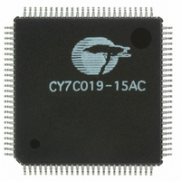
CY7C019-15AC Cypress Semiconductor Corp, CY7C019-15AC Datasheet

CY7C019-15AC
Specifications of CY7C019-15AC
Available stocks
Related parts for CY7C019-15AC
CY7C019-15AC Summary of contents
Page 1
... True Dual-Ported memory cells which allow simulta- neous access of the same memory location • 64K x 8 organization (CY7C008) • 128K x 8 organization (CY7C009) • 64K x 9 organization (CY7C018) • 128K x 9 organization (CY7C019) • 0.35-micron CMOS for optimum speed/power [1] • High-speed access: 12 /15/20 ns • ...
Page 2
... Two ports are provided permitting independent, asynchronous ac- cess for reads and writes to any location in memory. The de- vices can be utilized as standalone 8/9-bit dual-port static RAMs or multiple devices can be combined in order to function as a 16/18-bit or wider master/slave dual-port static RAM ...
Page 3
... Typical Standby Current for I (mA) (Both ports TTL level) SB1 Typical Standby Current for I (mA) (Both ports CMOS level) SB3 Note: 6. This pin is NC for CY7C018. Document #: 38-06041 Rev. *A 100-Pin TQFP (Top View CY7C019 (128K x 9) CY7C018 (64K CY7C008/009 CY7C018/019 CY7C008/009 CY7C018/019 ...
Page 4
... Supply Voltage to Ground Potential ............... –0.3V to +7.0V DC Voltage Applied to Outputs in High Z State ............................................... –0.5V to +7.0V Notes: 7. Pulse width < 20 ns. 8. Industrial parts are available in CY7C009 and CY7C019 only. Document #: 38-06041 Rev. *A Chip Enable (CE is LOW when CE 1R Read/Write Enable Output Enable Address (A –A ...
Page 5
Electrical Characteristics Over the Operating Range Parameter Description V Output HIGH Voltage OH (V =Min –4.0 mA Output LOW Voltage OL (V =Min +4.0 mA Input HIGH Voltage IH V ...
Page 6
Capacitance Parameter Description C Input Capacitance IN C Output Capacitance OUT AC Test Loads and Waveforms 893 OUTPUT 347 (a) Normal Load (Load 1) AC Test Loads (Applicable to -12 ...
Page 7
Switching Characteristics Over the Operating Range Parameter Description READ CYCLE t Read Cycle Time RC t Address to Data Valid AA t Output Hold From Address Change OHA [13 LOW to Data Valid ACE t OE LOW to ...
Page 8
Switching Characteristics Over the Operating Range Parameter Description [18] BUSY TIMING t BUSY LOW from Address Match BLA t BUSY HIGH from Address Mismatch BHA t BUSY LOW from CE LOW BLC t BUSY HIGH from CE HIGH BHC t ...
Page 9
Switching Waveforms Read Cycle No. 1 (Either Port Address Access) ADDRESS t OHA DATA OUT PREVIOUS DATA VALID Read Cycle No. 2 (Either Port CE/OE Access DATA OUT I CC CURRENT I SB [21, 23, 24, 25] Read ...
Page 10
Switching Waveforms (continued) Write Cycle No. 1: R/W Controlled Timing ADDRESS OE [30 R/W NOTE 32 DATA OUT DATA IN Write Cycle No Controlled Timing ADDRESS [28 R/W DATA IN Notes: 26. ...
Page 11
Switching Waveforms (continued) Semaphore Read After Write Timing, Either Side A –A VALID ADRESS 0 2 SEM I R/W OE Timing Diagram of Semaphore Contention A – R/W L SEM L A – ...
Page 12
Switching Waveforms (continued) Timing Diagram of Read with BUSY (M/S=HIGH) ADDRESS R R/W R DATA ADDRESS L BUSY L DATA OUTL Write Timing with Busy Input (M/S=LOW) R/W BUSY Note: 38 LOW. ...
Page 13
Switching Waveforms (continued) Busy Timing Diagram No. 1 (CE Arbitration) CE Valid First: L ADDRESS L BUSY R CE ValidFirst: R ADDRESS L BUSY L Busy Timing Diagram No. 2 (Address Arbitration) ...
Page 14
Switching Waveforms (continued) Interrupt Timing Diagrams Left Side Sets INT : R ADDRESS WRITE FFFF (1FFFF for CY7C009/19 R/W L INT R [41] t INS Right Side Clears INT : R ADDRESS R/W R ...
Page 15
... I/O and address lines, and control signals (CE, OE, R/W). These control pins permit independent access for reads or writes to any location in memory. To handle simultaneous writes/reads to the same location, a BUSY pin is provided on each port. Two interrupt (INT) pins can be utilized for port-to-port communication. Two sema- phore (SEM) control pins are used for allocating shared resources ...
Page 16
Table 1. Non-Contending Read/Write Inputs CE R/W OE SEM Table 2. Interrupt Operation ...
Page 17
... CY7C018-12AC 15 CY7C018-15AC 20 CY7C018-20AC 128K x 9 Asynchronous Dual-Port SRAM Speed (ns) Ordering Code [1] 12 CY7C019-12AC 15 CY7C019-15AC 20 CY7C019-20AC CY7C019-20AI Document #: 38-06041 Rev. *A Package Name Package Type A100 100-Pin Thin Quad Flat Pack A100 100-Pin Thin Quad Flat Pack A100 100-Pin Thin Quad Flat Pack ...
Page 18
... Document #: 38-06041 Rev. *A © Cypress Semiconductor Corporation, 2002. The information contained herein is subject to change without notice. Cypress Semiconductor Corporation assumes no responsibility for the use of any circuitry other than circuitry embodied in a Cypress Semiconductor product. Nor does it convey or imply any license under patent or other rights. Cypress Semiconductor does not authorize its products for use as critical components in life-support systems where a malfunction or failure may reasonably be expected to result in significant injury to the user ...
Page 19
Document Title: CY7C008/009, CY7C018/019 64K/128K x 8/9 Dual Port Static RAM Document Number: 38-06041 Issue REV. ECN NO. Date ** 110189 09/29/01 *A 113542 04/15/02 Document #: 38-06041 Rev. *A Orig. of Change Description of Change SZV Change from Spec ...


