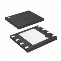
AT25DF641-MWH-Y Atmel, AT25DF641-MWH-Y Datasheet - Page 33

AT25DF641-MWH-Y
Manufacturer Part Number
AT25DF641-MWH-Y
Description
IC FLASH 64MBIT 100MHZ 8VDFN
Manufacturer
Atmel
Datasheet
1.AT25DF641-MWH-T.pdf
(56 pages)
Specifications of AT25DF641-MWH-Y
Format - Memory
FLASH
Memory Type
DataFLASH
Memory Size
64M (32K pages x 256 bytes)
Speed
100MHz
Interface
SPI, 3-Wire Serial
Voltage - Supply
2.7 V ~ 3.6 V
Operating Temperature
-40°C ~ 85°C
Package / Case
8-VDFN
Architecture
Sectored
Interface Type
SPI Serial
Supply Voltage (max)
3.6 V
Supply Voltage (min)
2.7 V
Maximum Operating Current
19 mA
Mounting Style
SMD/SMT
Organization
64 KB x 128
Cell Type
NOR
Density
64Mb
Access Time (max)
5ns
Boot Type
Not Required
Address Bus
1b
Operating Supply Voltage (typ)
3.3V
Operating Temp Range
-40C to 85C
Package Type
VDFN
Sync/async
Synchronous
Operating Temperature Classification
Industrial
Operating Supply Voltage (min)
2.7V
Operating Supply Voltage (max)
3.6V
Supply Current
19mA
Mounting
Surface Mount
Pin Count
8
Lead Free Status / RoHS Status
Lead free / RoHS Compliant
9.5.
3680F–DFLASH–4/10
If the device is powered-down during the OTP Security Register program cycle, then the contents of the 64-byte
user programmable portion of the OTP Security Register cannot be guaranteed and cannot be programmed
again.
The Program OTP Security Register command utilizes the internal 256-buffer for processing. Therefore, the
contents of the buffer will be altered from its previous state when this command is issued.
Figure 9-4.
Read OTP Security Register
The OTP Security Register can be sequentially read in a similar fashion to the Read Array operation up to the
maximum clock frequency specified by f
and the opcode of 77h must be clocked into the device. After the opcode has been clocked in, the three address
bytes must be clocked in to specify the starting address location of the first byte to read within the OTP Security
Register. Following the three address bytes, two dummy bytes must be clocked into the device before data can
be output.
After the three address bytes and the dummy bytes have been clocked in, additional clock cycles will result in
OTP Security Register data being output on the SO pin. When the last byte (00007Fh) of the OTP Security
Register has been read, the device will continue reading back at the beginning of the register (000000h). No
delays will be incurred when wrapping around from the end of the register to the beginning of the register.
Deasserting the
pin can be deasserted at any time and does not require that a full byte of data be read.
Figure 9-5.
SCK
SCK
SO
SO
CS
CS
SI
SI
Program OTP Security Register
Read OTP Security Register
CS
M S B
H IG H -IMP E DANC E
0
MS B
HIG H-IMP E DANC E
0
1
pin will terminate the read operation and put the SO pin into a high-impedance state. The
0
1
1
0
1
1
2
O P C O DE
0
2
1
OP C ODE
3
1
0
3
4
1
1
4
5
1
0
6
5
1
1
7
6
M S B
A
1
8
7
A
MS B
MAX
9
A
ADDR E S S B IT S A23-A0
ADDR E S S B IT S A23-A0
8
A
10 11
. To read the OTP Security Register, the
A
9
A
A
A
12
A
A
29 30
A
A
29 30
A
A
31 32
MS B
A
31 32
D
M S B
X
D
33
DAT A IN B Y T E 1
X
33
D
34
X
34
D
35
X
DO N'T C AR E
35
D
36
X
36
D
37 38
X
D
D
39
X
Atmel AT25DF641
X
X
CS
MS B
M S B
D
D
D
D
pin must first be asserted
DAT A IN B Y T E n
DAT A B Y T E 1
D
D
D
D
D
D
D
D
D
D
D
D
M S B
D
D
CS
33


