AT28LV010-20TU Atmel, AT28LV010-20TU Datasheet
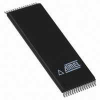
IC EEPROM 1MBIT 200NS 32TSOP

AT28LV010-20TU

Manufacturer Part Number
AT28LV010-20TU
Description
IC EEPROM 1MBIT 200NS 32TSOP
Manufacturer
Atmel
Datasheets

Specifications of AT28LV010-20TU

Format - Memory
EEPROMs - Parallel
Memory Type
EEPROM
Memory Size
1M (128K x 8)
Speed
200ns
Interface
Parallel
Voltage - Supply
3 V ~ 3.6 V
Operating Temperature
-40°C ~ 85°C
Package / Case
32-TSOP
Capacitance, Input
4 pF
Capacitance, Output
8 pF
Current, Input, Leakage
1 μA
Current, Operating
15 mA
Current, Output, Leakage
1
Data Retention
10 yrs.
Density
1M
Organization
128K×8
Package Type
TSOP
Power Dissipation
54 mW
Temperature, Operating
-40 to +85 °C
Time, Access
200 ns
Time, Address Hold
100
Voltage, Input, High
2 V
Voltage, Input, Low
0.8 V
Voltage, Output, High
2.4 V
Voltage, Output, Low
0.45 V
Voltage, Supply
3.3 V
Lead Free Status / RoHS Status
Lead free / RoHS Compliant

Available stocks

Company
Part Number
Manufacturer
Quantity
Price
Part Number:
AT28LV010-20TU
Manufacturer:
ATMEL
Quantity:
5 510
Part Number:
AT28LV010-20TU
Manufacturer:
AVER
Quantity:
5 510
Part Number:
AT28LV010-20TU
Manufacturer:
ATMEL/爱特梅尔
Quantity:
20 000
Features
1. Description
The AT28LV010 is a high-performance 3-volt only Electrically Erasable and Program-
mable Read-Only Memory. Its 1 megabit of memory is organized as 131,072 words by
8 bits. Manufactured with Atmel’s advanced nonvolatile CMOS technology, the device
offers access times to 200 ns with power dissipation of just 54 mW. When the device
is deselected, the CMOS standby current is less than 20 µA.
The AT28LV010 is accessed like a Static RAM for the read or write cycle without the
need for external components. The device contains a 128-byte page register to allow
writing of up to 128 bytes simultaneously. During a write cycle, the address and 1 to
128 bytes of data are internally latched, freeing the address and data bus for other
operations. Following the initiation of a write cycle, the device will automatically write
the latched data using an internal control timer. The end of a write cycle can be
detected by DATA polling of I/O7. Once the end of a write cycle has been detected a
new access for a read or write can begin.
Atmel’s 28LV010 has additional features to ensure high quality and manufacturability.
The device utilizes internal error correction for extended endurance and improved
data retention characteristics. Software data protection is implemented to guard
against inadvertent writes. The device also includes an extra 128 bytes of EEPROM
for device identification or tracking.
Single 3.3V ± 10% Supply
Fast Read Access Time – 200 ns
Automatic Page Write Operation
Fast Write Cycle Time
Low Power Dissipation
Hardware and Software Data Protection
DATA Polling for End of Write Detection
High Reliability CMOS Technology
JEDEC Approved Byte-Wide Pinout
Industrial and Automotive Temperature Ranges
Green (Pb/Halide-free) Packaging Option
– Internal Address and Data Latches for 128 Bytes
– Internal Control Timer
– Page Write Cycle Time – 10 ms Maximum
– 1 to 128-Byte Page Write Operation
– 15 mA Active Current
– 20 µA CMOS Standby Current
– Endurance: 10
– Data Retention: 10 Years
5
Cycles
1-Megabit
(128K x 8)
Low Voltage
Paged Parallel
EEPROMs
AT28LV010

Related parts for AT28LV010-20TU

AT28LV010-20TU Summary of contents

Page 1

... When the device is deselected, the CMOS standby current is less than 20 µA. The AT28LV010 is accessed like a Static RAM for the read or write cycle without the need for external components. The device contains a 128-byte page register to allow writing 128 bytes simultaneously ...

Page 2

... MHz mA 3.6V OUT 1 -100 µ 3. AT28LV010 AT28LV010-25 -40°C - 85°C 3.3V ± 10 Stresses beyond those listed under “Absolute Maximum Ratings” may cause permanent dam- age to the device. This is a stress rating only and functional operation of the device at these or any ...

Page 3

... OE may be delayed without impact ACC specified from whichever occurs first ( This parameter is characterized and is not 100% tested. AT28LV010 6 (1)(2)(3)( after the address transition without impact after the falling edge of CE without impact pF). L AT28LV010-20 Min Max Units 200 ns 200 ACC ...

Page 4

... Input Test Waveforms and Measurement Level 12. Output Test Load 13. Pin Capacitance ( MHz 25°C Symbol Typ OUT Note: 1. This parameter is characterized and is not 100% tested < Max 6 12 AT28LV010 Units Conditions OUT 7 ...

Page 5

... Chip Select Hold Time CH t Write Pulse Width ( Data Set-up Time Data, OE Hold Time DH OEH Note: 1. All write operations must be preceded by the SDP command sequence. 15. AC Write Waveforms 15.1 WE Controlled 15.2 CE Controlled AT28LV010 8 (1) Min Max Units 0 ns 100 200 ns 100 ...

Page 6

Software Protected Write Characteristics Symbol Parameter t Write Cycle Time WC t Address Set-up Time AS t Address Hold Time AH t Data Set-up Time DS t Data Hold Time DH t Write Pulse Width WP t Byte Load ...

Page 7

... These parameters are characterized and not 100% tested. 2. See AC Read Characteristics 22. Toggle Bit Waveforms Notes: 1. Toggling either both OE and CE will operate toggle bit. 2. Beginning and ending state of I/O6 will vary. 3. Any address location may be used but the address should not vary. AT28LV010 10 (1) Min ...

Page 8

... Die Products Reference Section: Parallel EEPROM Die Products (1) Ordering Code AT28LV010-20JI AT28LV010-20PI AT28LV010-20TI AT28LV010-25JI AT28LV010-25PI AT28LV010-25TI Ordering Code AT28LV010-20JU AT28LV010-20PU AT28LV010-20TU Package Type Package and Temperature Combinations JI, JU, PI, TI, TU, PU AT28LV010 Package Operation Range 32J Industrial 32P6 (-40° to 85° C) 32T 32J ...

Page 9

... This package conforms to JEDEC reference MO-142, Variation BD. 2. Dimensions D1 and E do not include mold protrusion. Allowable protrusion 0.15 mm per side and 0.25 mm per side. 3. Lead coplanarity is 0.10 mm maximum. TITLE 2325 Orchard Parkway San Jose, CA 95131 R AT28LV010 14 PIN 1 0º ~ 8º SEATING PLANE ...

Related keywords