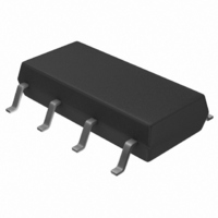
S-93C66BD0I-J8T1G Seiko Instruments, S-93C66BD0I-J8T1G Datasheet - Page 16

S-93C66BD0I-J8T1G
Manufacturer Part Number
S-93C66BD0I-J8T1G
Description
IC EEPROM 4KBIT 500KHZ 8SOP
Manufacturer
Seiko Instruments
Datasheet
1.S-93C46BD0I-T8T1G.pdf
(50 pages)
Specifications of S-93C66BD0I-J8T1G
Format - Memory
EEPROMs - Serial
Memory Type
EEPROM
Memory Size
4K (256 x 16)
Speed
500kHz
Interface
3-Wire Serial
Voltage - Supply
1.8 V ~ 5.5 V
Operating Temperature
-40°C ~ 85°C
Package / Case
8-SOP
Organization
256 K x 16
Interface Type
3-Wire
Maximum Clock Frequency
1 MHz
Supply Voltage (max)
5.5 V
Supply Voltage (min)
1.8 V
Maximum Operating Current
0.8 mA
Maximum Operating Temperature
+ 85 C
Mounting Style
SMD/SMT
Minimum Operating Temperature
- 40 C
Operating Supply Voltage
- 0.3 V, + 7 V
Lead Free Status / RoHS Status
Lead free / RoHS Compliant
Available stocks
Company
Part Number
Manufacturer
Quantity
Price
Part Number:
S-93C66BD0I-J8T1GE
Manufacturer:
SEIKO
Quantity:
20 000
16
3-WIRE SERIAL E
S-93C46B/56B/66B
4. 4 Writing to chip (WRAL)
CS
SK
DO
DI
To write the same 16-bit data to the entire memory address space, change CS to high, and then input the
WRAL instruction, an address, and 16-bit data following the start bit. Any address can be input. The
write operation starts when CS goes low. There is no need to set the data to 1 before writing. If the clocks
more than the specified number have been input, the clock pulse monitoring circuit cancels the WRAL
instruction. For details of the clock pulse monitoring circuit, refer to “
Write due to Erroneous Instruction Recognition ”.
DO
CS
SK
DI
1
2
1
PROM
2
0
2
0
0
3
0
3
0
High-Z
Figure 16 Chip Write Timing (S-93C56B, S-93C66B)
0
4
High-Z
4
1
5
Figure 15 Chip Write Timing (S-93C46B)
1
5
Seiko Instruments Inc.
6
6
7
7
6Xs
8
4Xs
8
9
9
10
D15
10
11
D15
12
25
D0
t
SV
t
CDS
27
D0
Function to Protect Against
t
PR
t
SV
t
CDS
Verify
busy
t
PR
ready
Verify
busy
Rev.7.0
Standby
High-Z
ready
t
HZ1
_00
Standby
High-Z
t
HZ1


