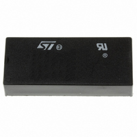
M48Z128Y-70PM1 STMicroelectronics, M48Z128Y-70PM1 Datasheet - Page 9

M48Z128Y-70PM1
Manufacturer Part Number
M48Z128Y-70PM1
Description
IC NVSRAM 1MBIT 70NS 32DIP
Manufacturer
STMicroelectronics
Type
NVSRAMr
Specifications of M48Z128Y-70PM1
Format - Memory
RAM
Memory Type
NVSRAM (Non-Volatile SRAM)
Memory Size
1M (128K x 8)
Speed
70ns
Interface
Parallel
Voltage - Supply
4.5 V ~ 5.5 V
Operating Temperature
0°C ~ 70°C
Package / Case
32-DIP (600 mil) Module
Data Bus Width
8 bit
Organization
128 Kb x 8
Interface Type
Parallel
Access Time
70 ns
Supply Voltage (max)
5.5 V
Supply Voltage (min)
4.5 V
Operating Current
105 mA
Maximum Operating Temperature
70 C
Minimum Operating Temperature
0 C
Mounting Style
Through Hole
Word Size
8b
Density
1Mb
Access Time (max)
70ns
Operating Supply Voltage (typ)
5V
Package Type
PMDIP
Operating Temperature Classification
Commercial
Operating Supply Voltage (max)
5.5V
Operating Supply Voltage (min)
4.5V
Operating Temp Range
0C to 70C
Pin Count
32
Mounting
Through Hole
Supply Current
105mA
Memory Configuration
128K X 8
Nvram Features
Internal Battery
Supply Voltage Range
4.5V To 5.5V
Memory Case Style
PMDIP
No. Of Pins
32
Rohs Compliant
Yes
Lead Free Status / RoHS Status
Lead free / RoHS Compliant
Other names
497-2874-5
Available stocks
Company
Part Number
Manufacturer
Quantity
Price
Part Number:
M48Z128Y-70PM1
Manufacturer:
ST
Quantity:
20 000
WRITE Mode
The M48Z128/Y/V is in the WRITE Mode whenev-
er W and E are active. The start of a WRITE is ref-
erenced from the latter occurring falling edge of W
or E. A WRITE is terminated by the earlier rising
edge of W or E.
The addresses must be held valid throughout the
cycle. E or W must return high for minimum of
t
Figure 8. WRITE Enable Controlled, WRITE AC Waveforms
Note: Output Enable (G) = High.
Figure 9. Chip Enable Controlled, WRITE AC Waveforms
Note: Output Enable (G) = High.
EHAX
from E or t
A0-A16
E
W
DQ0-DQ7
A0-A16
E
W
DQ0-DQ7
WHAX
from W prior to the initiation
tAVEL
tAVEL
tAVWL
tAVWL
tWLQZ
tAVWH
tAVEH
tWLWH
tAVAV
VALID
tAVAV
VALID
tELEH
of another READ or WRITE cycle. Data-in must be
valid t
valid for t
kept high during WRITE cycles to avoid bus con-
tention; although, if the output bus has been acti-
vated by a low on E and G, a low on W will disable
the outputs t
tDVEH
DVWH
tDVWH
DATA INPUT
WHDX
M48Z128, M48Z128Y, M48Z128V*
DATA INPUT
tWHDX
prior to the end of WRITE and remain
WLQZ
or t
after W falls.
EHDX
tEHDX
tWHQX
afterward. G should be
tEHAX
tWHAX
AI01198
AI01199
9/21


