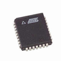
AT49LH004-33JC SL383 Atmel, AT49LH004-33JC SL383 Datasheet - Page 12

AT49LH004-33JC SL383
Manufacturer Part Number
AT49LH004-33JC SL383
Description
IC FLASH 4MBIT 33MHZ 32PLCC
Manufacturer
Atmel
Datasheet
1.AT49LH004-33JC.pdf
(40 pages)
Specifications of AT49LH004-33JC SL383
Format - Memory
FLASH
Memory Type
FLASH
Memory Size
4M (512K x 8)
Speed
33MHz
Interface
Parallel
Voltage - Supply
3 V ~ 3.6 V
Operating Temperature
0°C ~ 85°C
Package / Case
32-PLCC
Lead Free Status / RoHS Status
Contains lead / RoHS non-compliant
7.6
7.6.1
7.6.2
12
LPC Memory Cycles
AT49LH004
Start Field
CYCTYPE + DIR (Cycle Type And Direction) Field
A valid LPC memory cycle begins with the host driving the FWH4/LFRAME signal low for one
or more clock cycles. While the FWH4/LFRAME signal is low, a valid START value of 0000b
must be driven on the FWH/LAD[3:0] pins. Following the START field, a CYCTYPE + DIR
(Cycle Type and Direction) field must be sent to the device to indicate the type of cycle (e.g.,
memory access, I/O access, etc.) and the direction (read or write) of the transfer. After the
CYCTYPE + DIR field has been sent, the 8-clock MADDR (Memory Address) field must be
sent to the device to provide the 32-bit starting address location of where to begin reading or
writing in the memory.
Figure 7-4.
This 1-clock field indicates the start of a cycle. It is valid on the last clock that FWH4/LFRAME
is sampled low. The start field that is used for an LPC cycle is 0000b. If the start field that is
sampled is not 0000b, then the cycle attempted is not an LPC memory cycle. It may be a valid
FWH memory cycle that the device will attempt to decode.
This 1-clock field is used to indicate the type of cycle and the direction of the transfer to be per-
formed. Of the four bits placed on the FWH/LAD[3:0] pins, bits[3:2] must be 01b to indicate
that the transfer will be a memory cycle. Values other than 01b, which may be used to specify
an I/O cycle or a DMA cycle for other components in the system, will cause the device to enter
standby mode when the FWH4/LFRAME pin is brought high and no internal operation is in
progress. The FWH/LAD[3:0] pins will also be placed in a high-impedance state.
Bit[1] is used to determine the direction of the transfer. 0 is used to indicate a read, and 1 is
used to indicate a write. Bit[0] is ignored and reserved for future use.
valid CYCTYPE + DIR fields that the device will respond to.
Table 7-5.
FWH4/LFRAME
FWH/LAD[3:0]
FWH/LAD[3:0]
010xb
011xb
CLK
LPC Memory Cycle Initiation and Addressing
Valid CYCTYPE + DIR Values
Cycle Type
LPC Memory Read
LPC Memory Write
START
CYCTYPE
+ DIR
MADDR MADDR MADDR
MADDR
MADDR MADDR MADDR MADDR
Table 7-5
3383D–FLASH–6/05
details the two


