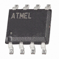
AT45DB021D-SSH-B Atmel, AT45DB021D-SSH-B Datasheet - Page 9

AT45DB021D-SSH-B
Manufacturer Part Number
AT45DB021D-SSH-B
Description
IC FLASH 2MBIT 66MHZ 8SOIC
Manufacturer
Atmel
Specifications of AT45DB021D-SSH-B
Format - Memory
FLASH
Memory Type
DataFLASH
Memory Size
2M (1024 pages x 264 bytes)
Speed
66MHz
Interface
SPI, RapidS
Voltage - Supply
2.7 V ~ 3.6 V
Operating Temperature
-40°C ~ 85°C
Package / Case
8-SOIC (3.9mm Width)
Architecture
Sectored
Interface Type
SPI
Supply Voltage (max)
3.6 V
Supply Voltage (min)
2.7 V
Maximum Operating Current
15 mA
Mounting Style
SMD/SMT
Organization
32 KB x 8
Memory Configuration
1024 Pages X 264 Bytes
Clock Frequency
66MHz
Supply Voltage Range
2.7V To 3.6V
Memory Case Style
SOIC
Rohs Compliant
Yes
Lead Free Status / RoHS Status
Lead free / RoHS Compliant
Other names
AT45DB021D-SSH
AT45DB021D-SSH
AT45DB021D-SSU
AT45DB021D-SSU
AT45DB021D-SSH
AT45DB021D-SSU
AT45DB021D-SSU
3638J–DFLASH–5/10
5.7
the binary page size (25-bytes), an opcode of 7CH must be loaded into the device, followed by three address bytes
comprised of six don’t care bits and seven page address bits (A17 - A11) and 11 don’t care bits. To perform a
sector 1-seven erase, the opcode 7CH must be loaded into the device, followed by three address bytes comprised
of six don’t care bit and three page address bits (A17 - A15) and 16 don’t care bits. The page address bits are used
to specify any valid address location within the sector which is to be erased. When a low-to-high transition occurs
on the CS pin, the part will erase the selected sector. The erase operation is internally self-timed and should take
place in a maximum time of t
Table 5-2.
Chip Erase
The entire main memory can be erased at one time by using the Chip Erase command.
To execute the Chip Erase command, a 4-byte command sequence C7H, 94H, 80H and 9AH must be clocked into
the device. Since the entire memory array is to be erased, no address bytes need to be clocked into the device,
and any data clocked in after the opcode will be ignored. After the last bit of the opcode sequence has been
clocked in, the CS pin can be deasserted to start the erase process. The erase operation is internally self-timed
and should take place in a time of t
The Chip Erase command will not affect sectors that are protected or locked down; the contents of those sectors
will remain unchanged. Only those sectors that are not protected or locked down will be erased.
The WP pin can be asserted while the device is erasing, but protection will not be activated until the internal erase
cycle completes.
Table 5-3.
Figure 5-1.
Command
Chip Erase
CS
SI
PA9/
A17
0
0
0
1
1
•
•
•
Each transition
represents 8 bits
PA8/
A16
Sector Erase Addressing
Chip Erase Command
Chip Erase
0
0
1
0
1
•
•
•
Opcode
Byte 1
PA7/
A15
0
0
1
0
1
•
•
•
Opcode
SE
Byte 2
. During this time, the status register will indicate that the part is busy.
PA6/
A14
CE
X
X
X
0
0
•
•
•
. During this time, the Status Register will indicate that the device is busy.
Opcode
Byte 3
Byte 1
C7H
PA5/
A13
X
X
X
0
0
•
•
•
Opcode
Byte 4
PA4/
A12
X
X
X
0
0
Byte 2
•
•
•
94H
PA3/
A11
X
X
X
0
1
•
•
•
Byte 3
80H
PA2/
A10
Atmel AT45DB021D
X
X
X
X
X
•
•
•
PA1/
Byte 4
A9
9AH
X
X
X
X
X
•
•
•
PA0/
A8
X
X
X
X
X
•
•
•
Sector
0a
0b
5
6
7
•
•
•
9


