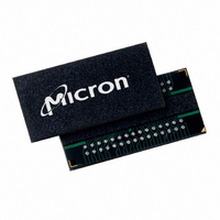
MT47H64M8CB-37E IT:B Micron Technology Inc, MT47H64M8CB-37E IT:B Datasheet - Page 103

MT47H64M8CB-37E IT:B
Manufacturer Part Number
MT47H64M8CB-37E IT:B
Description
IC DDR2 SDRAM 512MBIT 60FBGA
Manufacturer
Micron Technology Inc
Type
DDR2 SDRAMr
Datasheet
1.MT47H64M8CB-37E_ITB.pdf
(139 pages)
Specifications of MT47H64M8CB-37E IT:B
Format - Memory
RAM
Memory Type
DDR2 SDRAM
Memory Size
512M (64M x 8)
Speed
3.75ns
Interface
Parallel
Voltage - Supply
1.7 V ~ 1.9 V
Operating Temperature
-40°C ~ 85°C
Package / Case
60-FBGA
Organization
64Mx8
Density
512Mb
Address Bus
16b
Access Time (max)
500ps
Maximum Clock Rate
533MHz
Operating Supply Voltage (typ)
1.8V
Package Type
FBGA
Operating Temp Range
-40C to 85C
Operating Supply Voltage (max)
1.9V
Operating Supply Voltage (min)
1.7V
Supply Current
145mA
Pin Count
60
Mounting
Surface Mount
Operating Temperature Classification
Industrial
Lead Free Status / RoHS Status
Lead free / RoHS Compliant
- Current page: 103 of 139
- Download datasheet (10Mb)
Figure 53: READ-to-PRECHARGE – BL = 4
Figure 54: READ-to-PRECHARGE – BL = 8
PDF: 09005aef82f1e6e2
Rev. M 9/08 EN
Notes:
Notes:
not be issued until
the access of the last data elements.
Examples of READ-to-PRECHARGE for BL = 4 are shown in Figure 53 (page 103) and in
Figure 54 (page 103) for BL = 8. The delay from READ-to-PRECHARGE period to the
same bank is AL + BL/2 - 2CK + MAX (
of the two.
DQS, DQS#
DQS, DQS#
Command
Command
Address
Address
1. RL = 4 (AL = 1, CL = 3); BL = 4.
2.
3. Shown with nominal
1. RL = 4 (AL = 1, CL = 3); BL = 8.
2.
3. Shown with nominal
CK#
A10
DQ
CK#
A10
CK
DQ
CK
t
t
RTP ≥ 2 clocks.
RTP ≥ 2 clocks.
Bank a
Bank a
READ
READ
T0
T0
AL + BL/2 - 2CK + MAX ( t RTP/ t CK or 2CK)
AL = 1
AL = 1
First 4-bit
prefetch
prefetch
NOP
AL + BL/2 - 2CK + MAX ( t RTP/ t CK or 2CK)
4-bit
T1
≥ t RAS (MIN)
NOP
T1
t
RP is met. However, part of the row precharge time is hidden during
≥t RAS (MIN)
≥ t RTP (MIN)
NOP
T2
t
t
AC,
AC,
NOP
CL = 3
T2
103
Second 4-bit
t
t
DQSCK, and
DQSCK, and
CL = 3
prefetch
≥ t RC (MIN)
≥t RC (MIN)
NOP
T3
Bank a
Valid
PRE
T3
≥t RTP (MIN)
t
RTP/
Micron Technology, Inc. reserves the right to change products or specifications without notice.
NOP
T4
t
DO
t
DQSQ.
DQSQ.
512Mb: x4, x8, x16 DDR2 SDRAM
NOP
t
T4
CK or 2 × CK) where MAX means the larger
≥ t RP (MIN)
DO
DO
Bank a
Valid
PRE
T5
DO
DO
NOP
T5
Transitioning Data
Transitioning Data
DO
DO
NOP
T6
≥t RP (MIN)
DO
DO
Bank a
Valid
ACT
T6
DO
© 2004 Micron Technology, Inc. All rights reserved.
NOP
T7
DO
Don’t Care
Don’t Care
DO
NOP
T7
Bank a
Valid
ACT
T8
READ
Related parts for MT47H64M8CB-37E IT:B
Image
Part Number
Description
Manufacturer
Datasheet
Request
R

Part Number:
Description:
IC DDR2 SDRAM 512MBIT 3NS 60FBGA
Manufacturer:
Micron Technology Inc
Datasheet:

Part Number:
Description:
IC DDR2 SDRAM 512MBIT 5NS 60FBGA
Manufacturer:
Micron Technology Inc
Datasheet:

Part Number:
Description:
IC DDR2 SDRAM 512MBIT 60BGA
Manufacturer:
Micron Technology Inc

Part Number:
Description:
IC DDR2 SDRAM 512MBIT 60BGA
Manufacturer:
Micron Technology Inc

Part Number:
Description:
IC DDR2 SDRAM 512MBIT 60FBGA
Manufacturer:
Micron Technology Inc

Part Number:
Description:
IC DDR2 SDRAM 512MBIT 5NS 60FBGA
Manufacturer:
Micron Technology Inc

Part Number:
Description:
IC DDR2 SDRAM 512MBIT 5NS 60FBGA
Manufacturer:
Micron Technology Inc

Part Number:
Description:
IC DDR2 SDRAM 512MBIT 60FBGA
Manufacturer:
Micron Technology Inc

Part Number:
Description:
IC DDR2 SDRAM 512MBIT 60FBGA
Manufacturer:
Micron Technology Inc

Part Number:
Description:
IC DDR2 SDRAM 512MBIT 60FBGA
Manufacturer:
Micron Technology Inc

Part Number:
Description:
IC DDR2 SDRAM 512MBIT 60FBGA
Manufacturer:
Micron Technology Inc

Part Number:
Description:
IC DDR2 SDRAM 512MBIT 3NS 60FBGA
Manufacturer:
Micron Technology Inc

Part Number:
Description:
IC DDR2 SDRAM 512MBIT 5NS 60FBGA
Manufacturer:
Micron Technology Inc

Part Number:
Description:
IC SDRAM 64MBIT 133MHZ 54TSOP
Manufacturer:
Micron Technology Inc
Datasheet:

Part Number:
Description:
IC SDRAM 64MBIT 5.5NS 86TSOP
Manufacturer:
Micron Technology Inc
Datasheet:


