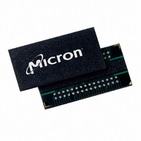
MT47H64M8CB-37E IT:B Micron Technology Inc, MT47H64M8CB-37E IT:B Datasheet - Page 33

MT47H64M8CB-37E IT:B
Manufacturer Part Number
MT47H64M8CB-37E IT:B
Description
IC DDR2 SDRAM 512MBIT 60FBGA
Manufacturer
Micron Technology Inc
Type
DDR2 SDRAMr
Datasheet
1.MT47H64M8CB-37E_ITB.pdf
(139 pages)
Specifications of MT47H64M8CB-37E IT:B
Format - Memory
RAM
Memory Type
DDR2 SDRAM
Memory Size
512M (64M x 8)
Speed
3.75ns
Interface
Parallel
Voltage - Supply
1.7 V ~ 1.9 V
Operating Temperature
-40°C ~ 85°C
Package / Case
60-FBGA
Organization
64Mx8
Density
512Mb
Address Bus
16b
Access Time (max)
500ps
Maximum Clock Rate
533MHz
Operating Supply Voltage (typ)
1.8V
Package Type
FBGA
Operating Temp Range
-40C to 85C
Operating Supply Voltage (max)
1.9V
Operating Supply Voltage (min)
1.7V
Supply Current
145mA
Pin Count
60
Mounting
Surface Mount
Operating Temperature Classification
Industrial
Lead Free Status / RoHS Status
Lead free / RoHS Compliant
Table 10: DDR2 Idd Specifications and Conditions (Continued)
Notes: 1–7 apply to the entire table
PDF: 09005aef82f1e6e2
Rev. M 9/08 EN
Parameter/Condition
Operating burst write current:All banks
open, continuous burst writes; BL = 4, CL =
CL (Idd), AL = 0;
MAX (Idd),
is HIGH between valid commands; address
bus inputs are switching; Data bus inputs are
switching
Operating burst read current: All banks
open, continuous burst reads, Iout = 0mA;
BL = 4, CL = CL (Idd), AL = 0;
t
HIGH, CS# is HIGH between valid commands;
address bus inputs are switching; Data bus in-
puts are switching
Burst refresh current:
fresh command at every
CKE is HIGH, CS# is HIGH between valid com-
mands; Other control and address bus inputs
are switching; Data bus inputs are switching
Self refresh current: CK and CK# at 0V;
CKE ≤ 0.2V; Other control and address bus
inputs are floating; Data bus inputs are float-
ing
Operating bank interleave read current:
All bank interleaving reads, Iout = 0mA; BL =
4, CL = CL (Idd), AL =
(Idd);
t
CS# is HIGH between valid commands; ad-
dress bus inputs are stable during deselects;
Data bus inputs are switching; See Idd7 Con-
ditions (page 31) for details
RAS =
RRD (Idd),
t
CK =
t
RAS MAX (Idd),
t
t
t
RCD =
RP =
CK (Idd),
t
CK =
t
RP (Idd); CKE is HIGH, CS#
t
RCD (Idd); CKE is HIGH,
t
t
Notes:
RCD (Idd) - 1 x
t
RC =
CK (Idd),
t
t
RP =
CK =
t
RFC (Idd) interval;
t
RC (Idd),
t
CK =
t
t
RP (Idd); CKE is
1. Idd specifications are tested after the device is properly initialized. 0°C ≤ T
2. Vdd = +1.8V ±0.1V, VddQ = +1.8V ±0.1V, VddL = +1.8V ±0.1V, Vref = VddQ/2.
3. Idd parameters are specified with ODT disabled.
4. Data bus consists of DQ, DM, DQS, DQS#, RDQS, RDQS#, LDQS, LDQS#, UDQS, and
5. Definitions for Idd conditions:
CK (Idd); re-
t
RAS =
UDQS#. Idd values must be met with all combinations of EMR bits 10 and 11.
t
LOW
HIGH
Stable
CK (Idd),
t
t
CK
RRD =
t
RAS
Symbol
Vin ≤ Vil(AC) MAX
Vin ≥ Vih(AC) MIN
Inputs stable at a HIGH or LOW level
Idd4W
Idd4R
Idd6L
Idd5
Idd6
Idd7
Configuration
33
x4, x8, x16
Electrical Specifications – Idd Parameters
x4, x8
x4, x8
x4, x8
x4, x8
x16
x16
x16
x16
Micron Technology, Inc. reserves the right to change products or specifications without notice.
512Mb: x4, x8, x16 DDR2 SDRAM
-25E/
195
295
205
275
230
230
300
370
-25
7
3
-3E/-3
170
250
180
235
180
185
240
350
7
3
© 2004 Micron Technology, Inc. All rights reserved.
-37E
140
205
145
195
170
175
225
340
7
3
115
160
115
155
165
170
220
340
-5E
7
3
C
≤ +85°C.
Units
mA
mA
mA
mA
mA


