MT48H8M16LFB4-8 IT:J TR Micron Technology Inc, MT48H8M16LFB4-8 IT:J TR Datasheet
MT48H8M16LFB4-8 IT:J TR
Specifications of MT48H8M16LFB4-8 IT:J TR


Related parts for MT48H8M16LFB4-8 IT:J TR


MT48H8M16LFB4-8 IT:J TR Summary of contents
Page 1
Mobile SDRAM MT48H8M16LF – 2 Meg banks MT48H4M32LF – 1 Meg banks Features • Vdd/Vddq = 1.7–1.95V • Fully synchronous; all signals registered on positive edge of system clock • Internal, pipelined ...
Page 2
Table of Contents Features . . . . . . . . . . . . . . . . . . . . . . . . . . . . . . . . . . . . ...
Page 3
List of Figures Figure 1: Part Numbering ...
Page 4
List of Tables Table 1: Configuration Addressing . . . . . . . . . . . . . . . . . . . . . . . . . . . . . . . . . ...
Page 5
... Addressing LF = Mobile standard addressing General Description The 128Mb Mobile SDRAM is a high-speed CMOS, dynamic random access memory containing 134,217,728 bits internally configured as a quad-bank DRAM with a synchronous interface (all signals are registered on the positive edge of the clock signal, CLK). Each of the x16’s 33,554,432-bit banks is organized as 4096 rows by 512 columns by 16 bits. Each of the x32’ ...
Page 6
... BA0, BA1 register PDF: 09005aef832ff1ea/Source: 09005aef832ff1ac 128mb_mobile_sdram_y35m__2.fm - Rev. E 4/09 EN 128Mb: 8 Meg x 16, 4 Meg x 32 Mobile SDRAM Bank 0 Row Row address Bank 0 address MUX memory latch and decoder Sense amplifiers I/O gating 2 DQM mask logic Bank read data latch control write drivers ...
Page 7
... Address Address BA0, BA1 register PDF: 09005aef832ff1ea/Source: 09005aef832ff1ac 128mb_mobile_sdram_y35m__2.fm - Rev. E 4/09 EN 128Mb: 8 Meg x 16, 4 Meg x 32 Mobile SDRAM Bank 0 Row- row- address address memory MUX latch and decode Sense amplifiers I/O gating 2 DQM mask logic Bank read data latch control write drivers ...
Page 8
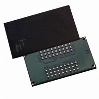
Ball Assignments Figure 4: 54-Ball VFBGA (Top View Notes: 1. The E2 pin must be connected to Vss, Vssq, or left floating. PDF: 09005aef832ff1ea/Source: 09005aef832ff1ac 128mb_mobile_sdram_y35m__2.fm - Rev. E 4/09 EN ...
Page 9
Figure 5: 90-Ball VFBGA (Top View Notes: 1. The K2 pin must be connected to Vss, Vssq, or left floating. PDF: 09005aef832ff1ea/Source: 09005aef832ff1ac 128mb_mobile_sdram_y35m__2.fm - ...
Page 10
... Address inputs: Addresses are sampled during the ACTIVE command (row) and READ/WRITE command (column; with A10 defining auto precharge) to select one location out of the memory array in the respective bank. A10 is sampled during a PRECHARGE command to determine whether all banks are to be precharged (A10 HIGH) or bank selected by BA0, BA1. The address inputs also provide the op-code during a LOAD MODE REGISTER command ...
Page 11
Table 3: VFBGA Ball Descriptions (continued) 54-Ball VFBGA 90-Ball VFBGA A7, B3, C7, D3 B2, B7, C9, D9, E1, L1, M9, N9, P2, P7 A3, B7, C3, D7 B3, B8, C1, D1, E9, L9, M1, N1, P3, P8 A9, E7, ...
Page 12
Package Dimensions Figure 6: 54-Ball VFBGA (8mm x 8mm) Seating plane A 0.1 A 54X Ø0.45 Dimensions apply to solder balls post-reflow. Pre- reflow balls are Ø0.42 on Ø0.4 SMD ball pads. 3.2 6.4 0.8 TYP Exposed ...
Page 13
Figure 7: 90-Ball VFBGA (8mm x 13mm) Seating plane A 0 ±0.1 90X Ø0.45 Dimensions apply to solder balls post- reflow. Pre-reflow balls are Ø0. Ø0.4 SMD ball pads. 5.6 11.2 0.8 TYP 3.2 ...
Page 14
Electrical Specifications Absolute Maximum Ratings Stresses greater than those listed in Table 4 may cause permanent damage to the device. This is a stress rating only, and functional operation of the device at these or any other conditions above those ...
Page 15
Table 7: Idd Specifications and Conditions (x16) Note 1 applies to all parameters and conditions; notes appear on page 16; Vdd/Vddq = 1.70–1.95V Parameter/Condition Operating current: Active mode; burst = 1; READ or WRITE; Standby current: Power-down mode; All banks ...
Page 16
Table 9: Idd7 Specifications and Conditions (x16 and x32) Notes and 10 apply to all conditions and parameters; Vdd/Vddq = 1.70–1.95V Parameter/Condition Self refresh CKE = LOW (MIN); Address and control inputs ...
Page 17
Figure 8: Typical Self Refresh Current vs. Temperature 120 Full array 1/2 array 100 1/4 array 1/8 array 1/16 array –50 –40 –30 PDF: 09005aef832ff1ea/Source: 09005aef832ff1ac 128mb_mobile_sdram_y35m__2.fm - Rev. E 4/09 EN 128Mb: 8 Meg ...
Page 18
Table 10: Electrical Characteristics and Recommended AC Operating Conditions Notes 1–5 apply to all parameters; notes appear on page 19 Parameter Access time from CLK (positive edge) Address hold time Address setup time CLK high-level width CLK low-level width Clock ...
Page 19
Table 11: AC Functional Characteristics Notes 1–5 apply to all parameters; notes appear on page 19 Parameter Last data-in to burst STOP command READ/WRITE command to READ/WRITE command Last data-in to new READ/WRITE command CKE to clock disable or power-down ...
Page 20
Required clocks are specified by JEDEC functionality and are not dependent on any timing parameter. 13. Timing is specified by 14. Timing is specified by rate. 15. Timing is specified by 16. Based on Table 12: Target Output Drive ...
Page 21
Table 13: Target Output Drive Characteristics (three-quarter strength) Notes 1–2 apply to all values; characteristics are specified under best and worst process variations/conditions Voltage (V) 0.00 0.10 0.20 0.30 0.40 0.50 0.60 11.76 0.70 13.72 0.80 15.68 0.85 16.66 0.90 ...
Page 22
Table 14: Target Output Drive Characteristics (one-half strength) Notes 1–3 apply to all values; characteristics are specified under best and worst process variations/conditions Voltage (V) 0.00 0.10 0.20 0.30 0.40 0.50 0.60 0.70 0.80 10.16 0.85 10.80 0.90 10.80 0.95 ...
Page 23
Revision History: Device Rev. E, Productions ...
Page 24
... Precharging one bank while accessing one of the other three banks will hide the precharge cycles and provide seamless high-speed, random- access operation. Mobile SDRAM is designed to operate in 1.8V memory systems. An auto refresh mode is provided, along with power-saving, power-down, and deep power-down modes. All inputs and outputs are LVTTL-compatible. ...
Page 25
Commands Table 15 provides a quick reference of available commands. A written description of each command follows the table. Three additional Truth Tables appear on pages 30–34; these tables provide current state/next state information. Table 15: Truth Table – Commands ...
Page 26
COMMAND INHIBIT The COMMAND INHIBIT function prevents new commands from being executed by the SDRAM, regardless of whether the CLK signal is enabled. The SDRAM is effectively deselected. Operations already in progress are not affected. NO OPERATION (NOP) The NO ...
Page 27
... Input data appearing on the DQ is written to the memory array subject to the DQM input logic level appearing coincident with the data given DQM signal is registered LOW, the corresponding data is written to memory ...
Page 28
Figure 11: WRITE Command CLK CKE RAS# CAS# WE# Address A10 BA0, BA1 Notes enable auto precharge, DIS AP = disable auto precharge PRECHARGE The PRECHARGE command is used to deactivate the open row in a ...
Page 29
Figure 12: PRECHARGE Command CLK CKE CS# RAS# CAS# WE# Address A10 BA0, BA1 BURST TERMINATE The BURST TERMINATE command is used to truncate either fixed-length or continuous page bursts. The most recently registered READ or WRITE command prior to ...
Page 30
... DEEP POWER-DOWN (DPD) The DEEP POWER-DOWN (DPD) command is used to enter deep power-down mode, achieving maximum power reduction by eliminating the power to the memory array. To enter DPD, all banks must be idle. While CKE is LOW, hold CS# and WE# LOW, and hold RAS# and CAS# HIGH at the rising edge of the clock. To exit DPD, assert CKE HIGH. ...
Page 31
Table 17 on page 32. Precharging: Row activating: Read with auto precharge enabled: Write with auto precharge enabled: 5. The states listed ...
Page 32
Table 17: Truth Table – Current State Bank n, Command to Bank m Notes 1–6 apply to all parameters in this table; notes appear below table Current State CS# Any Idle L Row activating, active, or precharging ...
Page 33
All states and sequences not shown are illegal or reserved. 7. READs or WRITEs to bank m listed in the Command/Action column include READs or WRITEs with auto precharge enabled and READs or WRITEs with auto precharge disabled. 8. ...
Page 34
Table 18: Truth Table – CKE Notes 1–4 apply to all parameters in this table; notes appear below table CKE CKE Current State n Power-down Self refresh Clock suspend Deep power-down L H Power-down Deep power-down Self ...
Page 35
When in the idle state, two AUTO REFRESH cycles must be performed. After the AUTO REFRESH cycles are complete, the SDRAM is ready for mode register programming. Because the mode register powers unknown state, it should be ...
Page 36
Register Definition Mode Register There are two mode registers in the Mobile SDRAM component, the mode register and the extended mode register (EMR). The mode register is illustrated in Figure 14 on page 37. The mode register defines the specific ...
Page 37
Figure 14: Mode Register Definition BA1 BA0 An Mn+2 Mn+1 Mn n+2 n Mode Register Definition Mn+2 Mn Base mode register 0 1 Reserved 1 0 Extended mode register 1 1 Reserved Write Burst Mode ...
Page 38
Burst Type Accesses within a given burst can be programmed to be either sequential or interleaved; this is referred to as the burst type and is selected via bit M3. The ordering of accesses within a burst is determined by ...
Page 39
Figure 15: CAS Latency Command Command Operating Mode The normal operating mode is selected by setting M7 and M8 to zero; the other combi- nations of values for M7 and M8 are reserved for future use. Reserved states should not ...
Page 40
... Partial-Array Self Refresh (PASR) For further power savings during self refresh, the PASR feature enables the controller to select the amount of memory to be refreshed during self refresh. The refresh options are: • Full array: banks and 3 • One-half array: banks 0 and 1 • ...
Page 41
... Drive strength should be selected based on the expected loading of the memory bus. There are four supported settings for the output drivers: 25Ω, 37Ω, 55Ω, and 80Ω internal impedance. These are full, three-quarter, one-half, and one-quarter drive strengths, respectively ...
Page 42
Timing Diagrams READs READ bursts are initiated with a READ command, as shown in Figure 10 on page 27. The starting column and bank addresses are provided with the READ command, and auto precharge is either enabled or disabled for ...
Page 43
Figure 18: Consecutive READ Bursts Command Address Command Address Notes: 1. Each READ command can be to any bank. DQM is LOW. PDF: 09005aef832ff1ea/Source: 09005aef832ff1ac sdr_mobile_sdram_cmd_op_timing_dia_fr10_08__3.fm - Rev. E 4/09 EN 128Mb: 8 Meg x 16, 4 Meg x 32 ...
Page 44
Figure 19: Random READ Accesses Command Address Command Address Notes: 1. Each READ command can be to any bank. DQM is LOW. Data from any READ burst can be truncated with a subsequent WRITE command, and data from a fixed-length ...
Page 45
The DQM signal must be de-asserted prior to the WRITE command (DQM latency is zero clocks for input buffers) to ensure that the written data is not masked. Figure 19 on page 44 shows the case where the clock frequency ...
Page 46
Figure 21: READ-to-WRITE With Extra Clock Cycle DQM Command Address Notes The READ command can be to any bank, and the WRITE command can be to any bank. Figure 22: READ-to-PRECHARGE Command Address Command Address Notes: ...
Page 47
Continuous-page READ bursts can be truncated with a BURST TERMINATE command and fixed-length READ bursts can be truncated with a BURST TERMINATE command, provided that auto precharge was not activated. The BURST TERMINATE command should be issued x cycles before ...
Page 48
Figure 24: Alternating Bank Read Accesses CLK t CKS t CKH CKE t CMS t CMH Command ACTIVE NOP t CMS DQM Row Address Enable auto ...
Page 49
Figure 25: READ Continuous Page Burst CLK CKS t CKH CKE t CMS t CMH Command ACTIVE NOP READ t CMS DQM Address Row Column m ...
Page 50
Figure 26: READ – DQM Operation CLK t CKS t CKH CKE t CMS t CMH Command ACTIVE NOP t CMS DQM Row Address Enable auto ...
Page 51
WRITEs WRITE bursts are initiated with a WRITE command, as shown in Figure 11 on page 28. The starting column and bank addresses are provided with the WRITE command and auto precharge is either enabled or disabled for that access. ...
Page 52
Figure 28: WRITE-to-WRITE Command Address Notes: 1. DQM is LOW. Each WRITE command may be to any bank. Data for any WRITE burst can be truncated with a subsequent READ command, and data for a fixed-length WRITE burst can be ...
Page 53
Figure 29: Random WRITE Cycles Command Address Notes: 1. Each WRITE command can be to any bank. DQM is LOW. Figure 30: WRITE-to-READ Command Address Notes: 1. The WRITE command can be to any bank, and the READ command can ...
Page 54
Figure 31: WRITE-to-PRECHARGE Command Address Command Address Notes this example DQM could remain LOW if the WRITE burst is a fixed length of two. Fixed-length WRITE bursts can be truncated with the ...
Page 55
Figure 32: Terminating a WRITE Burst Command Address Notes: 1. DQM is LOW. Figure 33: Alternating Bank Write Accesses CLK t CKS t CKH CKE t CMS t CMH Command ACTIVE NOP WRITE ...
Page 56
Figure 34: WRITE – Continuous Page Burst CLK CKS t CKH CKE t CMS t CMH Command ACTIVE NOP DQM Address Row Row A10 t ...
Page 57
Figure 35: WRITE – DQM Operation CLK t CKS t CKH CKE t CMS t CMH Command ACTIVE NOP DQM Address Row Row A10 ...
Page 58
A precharge of the bank/row that is addressed with the READ or WRITE command is automatically performed upon completion of the READ or WRITE burst, except in the continuous page burst mode, where auto precharge does not apply. In ...
Page 59
Figure 36: READ With Auto Precharge Interrupted by a READ CLK Command Bank n Internal states Bank m Address DQ Notes: 1. DQM is LOW. Figure 37: READ With Auto Precharge Interrupted by a WRITE CLK READ - AP Command ...
Page 60
Figure 38: READ With Auto Precharge CLK t CKS t CKH CKE t CMS t CMH Command ACTIVE NOP t CMS DQM Row Address Enable auto ...
Page 61
Figure 39: READ Without Auto Precharge CLK t CKS t CKH CKE t CMS t CMH Command ACTIVE NOP t CMS DQM Row Address Row A10 ...
Page 62
Figure 40: Single READ With Auto Precharge CLK t CKS t CKH CKE t CMS t CMH Command ACTIVE NOP DQM Address Row A10 Row ...
Page 63
Figure 41: Single READ Without Auto Precharge CLK t CKS t CKH CKE t CMS t CMH Command ACTIVE NOP t CMS DQM Address Row A10 ...
Page 64
Figure 42: WRITE With Auto Precharge Interrupted by a READ Command Internal States Address Notes: 1. DQM is LOW. Figure 43: WRITE With Auto Precharge Interrupted by a WRITE Command Internal States Address Notes: 1. DQM is LOW. PDF: 09005aef832ff1ea/Source: ...
Page 65
Figure 44: WRITE With Auto Precharge CLK t CKS t CKH CKE t CMS t CMH Command ACTIVE NOP t CMS DQM Address Row Column ...
Page 66
Figure 45: WRITE Without Auto Precharge CLK t CKS t CKH CKE t CMS t CMH Command ACTIVE NOP t CMS DQM Address Row Column ...
Page 67
Figure 46: Single WRITE With Auto Precharge CLK t CKS t CKH CKE t CMS t CMH Command ACTIVE NOP t CMS DQM Address Row Enable ...
Page 68
Figure 47: Single WRITE Without Auto Precharge CLK t CKS t CKH CKE t CMS t CMH Command ACTIVE NOP t CMS DQM Address Row A10 ...
Page 69
Figure 48: Auto Refresh Mode T0 T1 CLK t CK CKE t CKS t CKH t CMS t CMH Command PRECHARGE NOP DQM Address All banks A10 Single bank BA0, BA1 Bank(s) High ...
Page 70
The procedure for exiting self refresh requires a sequence of commands. First, CLK must be stable (stable clock is defined as a signal cycling within timing constraints specified for the clock ball) prior to CKE going back HIGH. After CKE ...
Page 71
Power-Down Power-down occurs if CKE is registered LOW coincident with a NOP or COMMAND INHIBIT when no accesses are in progress. If power-down occurs when all banks are idle, this mode is referred to as precharge power-down; if power-down occurs ...
Page 72
... Deep Power-Down Deep power-down mode is a maximum power-saving feature achieved by shutting off the power to the entire device memory array. Data on the memory array will not be retained after deep power-down mode is executed. Deep power-down mode is entered by having all banks idle, with CS# and WE# held LOW with RAS# and CAS# HIGH at the rising edge of the clock, while CKE is LOW ...
Page 73
Figure 52: Clock Suspend During READ Burst Internal clock Command Address Notes: 1. For this example greater, and DQM is LOW. PDF: 09005aef832ff1ea/Source: 09005aef832ff1ac sdr_mobile_sdram_cmd_op_timing_dia_fr10_08__3.fm - Rev. E 4/09 EN 128Mb: 8 Meg ...
Page 74
Figure 53: Clock Suspend Mode CLK t CKS CKE t CKS t CKH t CMS t CMH Command READ NOP t CMS t CMH DQM Column m Address t AS ...
Page 75
Revision History: Commands, Operations, and Timing Diagrams Revision History: Commands, Operations, and Timing Diagrams Update . . . . . . . . . . . . . . . . . . . . . . . . . ...