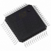
DSM2190F4V-15T6 STMicroelectronics, DSM2190F4V-15T6 Datasheet - Page 18

DSM2190F4V-15T6
Manufacturer Part Number
DSM2190F4V-15T6
Description
IC FLASH 2MBIT 150NS 52QFP
Manufacturer
STMicroelectronics
Datasheet
1.DSM2190F4V-15K6.pdf
(61 pages)
Specifications of DSM2190F4V-15T6
Format - Memory
FLASH
Memory Type
FLASH
Memory Size
2M (256K x 8)
Speed
150ns
Interface
Parallel
Voltage - Supply
3 V ~ 3.6 V
Operating Temperature
-40°C ~ 85°C
Package / Case
52-QFP
Operating Supply Voltage (typ)
3.3V
Operating Supply Voltage (min)
3V
Operating Supply Voltage (max)
3.6V
Operating Temp Range
-40C to 85C
Operating Temperature Classification
Industrial
Mounting
Surface Mount
Pin Count
52
Lead Free Status / RoHS Status
Lead free / RoHS Compliant
Other names
497-1323
Available stocks
Company
Part Number
Manufacturer
Quantity
Price
Company:
Part Number:
DSM2190F4V-15T6
Manufacturer:
STMicroelectronics
Quantity:
10 000
DSM2190F4
Instruction Sequences
An instruction sequence consists of a sequence of
specific write or read operations. Each byte written
to the device is received and sequentially decoded
and not executed as a standard write operation to
the memory array. The instruction sequence is ex-
ecuted when the correct number of bytes are prop-
erly
consecutive bytes is shorter than the time-out pe-
riod. Some instruction sequences are structured to
include read operations after the initial write oper-
ations.
The instruction sequence must be followed exact-
ly. Any invalid combination of instruction bytes or
time-out between two consecutive bytes while ad-
dressing Flash memory resets the device logic into
Read Array mode (Flash memory is read like a
ROM device). The device supports the instruction
sequences summarized in Table 5:
Flash memory:
These instruction sequences are detailed in Table
5. For efficient decoding of the instruction se-
quences, the first two bytes of an instruction se-
quence are the coded cycles and are followed by
an instruction byte or confirmation byte. The coded
cycles consist of writing the data AAh to address
XX555h during the first cycle and data 55h to ad-
dress XXAAAh during the second cycle. Address
signals A18-A12 are Don’t Care during the instruc-
tion sequence Write cycles. However, the appro-
priate
CSBOOT0-CSBOOT3 ) must be selected internal-
ly (active, which is logic 1).
Table 6. Status Bit Definition
Note: 1. X = Not guaranteed value, can be read either 1 or 0.
Reading the Erase/Program Status Bits. The
device provides several status bits to be used by
the DSP to confirm the completion of an Erase or
18/61
Functional Block
Erase memory by chip or sector
Suspend or resume sector erase
Program a Byte
Reset to Read Array mode
Read primary Flash Identifier value
Read Sector Protection Status
Flash Memory
2. DQ7-DQ0 represent the Data Bus bits, D7-D0.
received
internal
and
Sector
CSBOOT0-CSBOOT3
segment is selected)
Active (the desired
the
FS0-FS7, or
Select
time
between
( FS0-FS7
Polling
Data
DQ7
two
or
Toggle
DQ6
Flag
Reading Flash Memory
Under typical conditions, the DSP may read the
Flash memory using read operations just as it
would a ROM or RAM device. Alternately, the DSP
may use read operations to obtain status informa-
tion about a Program or Erase cycle that is cur-
rently in progress. Lastly, the DSP may use
instruction sequences to read special data from
these memory blocks. The following sections de-
scribe these read instruction sequences.
Read Memory Contents. Flash
placed in the Read Array mode after Power-up,
chip reset, or a Reset Flash memory instruction
sequence (see Table 5). The DSP can read the
memory contents of the Flash memory by using
read operations any time the read operation is not
part of an instruction sequence.
Read Main Flash Identifier. The
memory identifier is read with an instruction se-
quence composed of 4 operations: 3 specific write
operations and a read operation (see Table 5).
During the read operation, address bits A6, A1,
and A0 must be 0,0,1, respectively, and the appro-
priate internal Sector Select ( FS0-FS7 ) must be
active. The identifier is 0xE7. Not Applicable to
Secondary Flash.
Read Memory Sector Protection Status. The
Flash memory Sector Protection Status is read
with an instruction sequence composed of 4 oper-
ations: 3 specific write operations and a read oper-
ation (see Table 5). During the read operation,
address bits A6, A1, and A0 must be 0,1,0, re-
spectively, while internal Sector Select (FS0-FS7
or CSBOOT0-CSBOOT3) designates the Flash
memory sector whose protection has to be veri-
fied. The read operation produces 01h if the Flash
memory sector is protected, or 00h if the sector is
not protected.
The sector protection status can also be read by
the DSP accessing the Flash memory Protection
registers in csiop space. See the section entitled
“Flash Memory Sector Protect” for register defini-
tions.
Program cycle of Flash memory. These status bits
minimize the time that the DSP spends performing
these tasks and are defined in Table 6. The status
bits can be read as many times as needed.
Error
DQ5
Flag
DQ4
X
Erase
Time-
DQ3
out
DQ2
X
DQ1
memory
Main
X
DQ0
Flash
X
is


