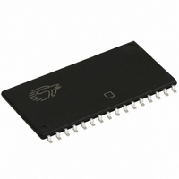
CY62128DV30LL-70ZI Cypress Semiconductor Corp, CY62128DV30LL-70ZI Datasheet

CY62128DV30LL-70ZI
Specifications of CY62128DV30LL-70ZI
Available stocks
Related parts for CY62128DV30LL-70ZI
CY62128DV30LL-70ZI Summary of contents
Page 1
... WE OE Note: 1. For best-practice recommendations, please refer to the Cypress application note “System Design Guidelines” on http://www.cypress.com. Cypress Semiconductor Corporation Document #: 38-05231 Rev. *H 1-Mb (128K x 8) Static RAM also has an automatic power-down feature that significantly reduces power consumption by 90% when addresses are not toggling ...
Page 2
... Min. Typ. CY62128DV30L 2.2 3.0 CY62128DV30LL Notes pins are not connected to the die. 3. DNU pins have to be left floating or tied to Vss to ensure proper application. 4. Typical values are included for reference only and are not guaranteed or tested. Typical values are measured at V Document #: 38-05231 Rev. *H ...
Page 3
Maximum Ratings (Above which the useful life may be impaired. For user guide- lines, not tested.) Storage Temperature ................................. –65°C to +150°C Ambient Temperature with Power Applied............................................. –55°C to +125°C Supply Voltage to Ground Potential .......................................................... −0.3V to 3.9V DC ...
Page 4
AC Test Loads and Waveforms OUTPUT 50 pF INCLUDING JIG AND SCOPE Parameters Data Retention Characteristics Parameter Description V V for Data Retention Data Retention Current CCDR [4] ...
Page 5
... At any given temperature and voltage condition and t transitions are measured when the outputs enter a high-impedance state. HZOE HZCE HZBE HZWE 12. The internal write time of the memory is defined by the overlap of WE, CE 13. Device is continuously selected HIGH for Read cycle. Document #: 38-05231 Rev. *H [9] CY62128DV30-55 Description Min. ...
Page 6
Switching Waveforms (continued) [11, 14, 15] Read Cycle No. 2 (OE Controlled) ADDRESS ACE OE t LZOE HIGH IMPEDANCE DATA OUT t LZCE SUPPLY CURRENT [12, 16, 17, 18] Write Cycle ...
Page 7
Switching Waveforms (continued) Write Cycle No Controlled ADDRESS DATA I/O Write Cycle No. 3 (WE Controlled, OE LOW) ADDRESS DON'T CARE DATA ...
Page 8
... CY62128DV30L-55ZI CY62128DV30LL-55ZI CY62128DV30LL-55ZXI CY62128DV30L-55ZAI CY62128DV30LL-55ZAI CY62128DV30LL-55ZAXI CY62128DV30L-55ZRI CY62128DV30LL-55ZRI CY62128DV30LL-55ZRXI 70 CY62128DV30L-70SI CY62128DV30LL-70SI CY62128DV30LL-70SXI CY62128DV30L-70ZI CY62128DV30LL-70ZI CY62128DV30LL-70ZXI CY62128DV30L-70ZAI CY62128DV30LL-70ZAI CY62128DV30LL-70ZAXI CY62128DV30L-70ZRI CY62128DV30LL-70ZRI Document #: 38-05231 Rev. *H Package Diagram Package Type 51-85081 32-lead SOIC 51-85081 32-lead SOIC 51-85081 32-lead SOIC (Pb-Free) 51-85056 32-lead TSOP Type 1 ...
Page 9
Package Diagrams 32 LD (450 Mil) SOIC 16 17 0.793[20.142] 0.817[20.751] 0.101[2.565] 0.111[2.819] 0.050[1.270] BSC. 0.014[0.355] 0.020[0.508] 32-Lead TSOP Type mm) (51-85056) Document #: 38-05231 Rev. *H 32-Lead (450-Mil) SOIC (51-85081) 1 0.546[13.868] 0.566[14.376] 0.440[11.176] DIMENSIONS ...
Page 10
... Document #: 38-05231 Rev. *H © Cypress Semiconductor Corporation, 2006. The information contained herein is subject to change without notice. Cypress Semiconductor Corporation assumes no responsibility for the use of any circuitry other than circuitry embodied in a Cypress product. Nor does it convey or imply any license under patent or other rights. Cypress products are not warranted nor intended to be used for medical, life support, life saving, critical control or safety applications, unless pursuant to an express written agreement with Cypress ...
Page 11
... Add 70-ns speed, updated ordering information CDY Changed Icc 1 MHz typ from 0 0.85 mA PCI Added Lead-Free Packages in Ordering Information Table SYT Changed address of Cypress Semiconductor Corporation on Page# 1 from “3901 North First Street” to “198 Champion Court” Corrected CE and CE waveforms on Write Cycle No.1 on Page Edited the Write Cycle No.1 switching waveform Data I/O to include Don’ ...


