EPCS16SI16N Altera, EPCS16SI16N Datasheet - Page 28
EPCS16SI16N
Manufacturer Part Number
EPCS16SI16N
Description
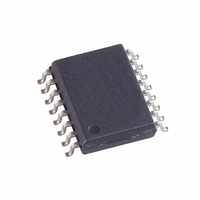
IC CONFIG DEVICE 16MBIT 16-SOIC
Manufacturer
Altera
Series
EPCSr
Specifications of EPCS16SI16N
Programmable Type
In System Programmable
Memory Size
16Mb
Voltage - Supply
3 V ~ 3.6 V
Operating Temperature
-40°C ~ 85°C
Package / Case
16-SOIC (0.300", 7.50mm Width)
Memory Type
Flash
Clock Frequency
20MHz
Supply Voltage Range
2.7V To 3.6V
Memory Case Style
SOIC
No. Of Pins
16
Operating Temperature Range
-40°C To +85°C
Rohs Compliant
Yes
Lead Free Status / RoHS Status
Lead free / RoHS Compliant
Other names
544-1240-5
EPCS16SI16
EPCS16SI16
Available stocks
Company
Part Number
Manufacturer
Quantity
Price
Company:

Part Number:
EPCS16SI16N
Manufacturer:
ALTERA
Quantity:
1 250
Company:
Part Number:
EPCS16SI16N
Manufacturer:
ALTERA44
Quantity:
540
Part Number:
EPCS16SI16N
Manufacturer:
ALTERA/阿尔特拉
Quantity:
20 000


3–28
Figure 3–19. Read Operation Timing
Configuration Handbook (Complete Two-Volume Set)
f
1
DCLK
DATA
ASDI
nCS
Add_Bit 0
Figure 3–19
operation.
Table 3–17
operation.
Table 3–17. Read Operation Parameters
Existing batches of EPCS1 and EPCS4 manufactured on 0.15 µm process geometry
support AS configuration up to 40 MHz. However, batches of EPCS1 and EPCS4
manufactured on 0.18 µm process geometry support only up to 20 MHz. EPCS16,
EPCS64, and EPCS128 are not affected.
For information about product traceability and transition date to differentiate
between 0.15 µm process geometry and 0.18 µm process geometry EPCS1 and EPCS4,
refer tothe Process Change Notification
Family.
f
t
t
t
t
RCLK
CH
CL
ODIS
nCLK2D
Symbol
t
nCLK2D
defines the serial configuration device timing parameters for read
Chapter 3: Serial Configuration Devices (EPCS1, EPCS4, EPCS16, EPCS64, and EPCS128) Data Sheet
Bit N
shows the timing waveform for the serial configuration device's read
Read clock frequency (from FPGA or
embedded processor) for read bytes
operation
DCLK high time
DCLK low time
Output disable time after read
Clock falling edge to data
Bit N 1
Parameter
PCN 0514: Manufacturing Changes on EPCS
t
CL
t
CH
Min
Bit 0
—
25
25
—
—
© December 2009
t
ODIS
Max
15
20
—
—
8
Timing Information
Altera Corporation
MHz
Unit
ns
ns
ns
ns
Related parts for EPCS16SI16N
Image
Part Number
Description
Manufacturer
Datasheet
Request
R

Part Number:
Description:
IC CONFIG DEVICE 1MBIT 8-SOIC
Manufacturer:
Altera
Datasheet:
Part Number:
Description:
IC CONFIG DEVICE 4MBIT 8-SOIC
Manufacturer:
Altera
Datasheet:
Part Number:
Description:
IC CONFIG DEVICE 4MBIT 8-SOIC
Manufacturer:
Altera
Datasheet:
Part Number:
Description:
IC CONFIG DEVICE 16MBIT 8-SOIC
Manufacturer:
Altera
Datasheet:

Part Number:
Description:
IC CONFIG DEVICE 64MBIT 16-SOIC
Manufacturer:
Altera
Datasheet:
Part Number:
Description:
IC CONFIG DEVICE 1MBIT 8-SOIC
Manufacturer:
Altera
Datasheet:

Part Number:
Description:
CYCLONE II STARTER KIT EP2C20N
Manufacturer:
Altera
Datasheet:


Part Number:
Description:
CPLD, EP610 Family, ECMOS Process, 300 Gates, 16 Macro Cells, 16 Reg., 16 User I/Os, 5V Supply, 35 Speed Grade, 24DIP
Manufacturer:
Altera Corporation
Datasheet:
Part Number:
Description:
CPLD, EP610 Family, ECMOS Process, 300 Gates, 16 Macro Cells, 16 Reg., 16 User I/Os, 5V Supply, 15 Speed Grade, 24DIP
Manufacturer:
Altera Corporation
Datasheet:
Part Number:
Description:
Manufacturer:
Altera Corporation
Datasheet:
Part Number:
Description:
CPLD, EP610 Family, ECMOS Process, 300 Gates, 16 Macro Cells, 16 Reg., 16 User I/Os, 5V Supply, 30 Speed Grade, 24DIP
Manufacturer:
Altera Corporation
Datasheet:
Part Number:
Description:
High-performance, low-power erasable programmable logic devices with 8 macrocells, 10ns
Manufacturer:
Altera Corporation
Datasheet: