EPCS4SI8 Altera, EPCS4SI8 Datasheet
EPCS4SI8
Specifications of EPCS4SI8
Available stocks


Related parts for EPCS4SI8


EPCS4SI8 Summary of contents
Page 1
... BP Microsystems, System General, and other vendors ■ Delivered with the memory array erased (all the bits set The term “serial configuration devices” used in this document refers to Altera EPCS1, EPCS4, EPCS16, EPCS64, and EPCS128. © December 2009 Altera Corporation 3. Serial Configuration Devices (EPCS1, EPCS4, EPCS16, EPCS64, and EPCS128) ® ...
Page 2
... Notes to Table 3–1: (1) To program these devices using Altera Programming Unit or Master Programming Unit, refer to (2) The EPCS device can be re-programmed in system with Byte Blaster II download cable or an external microprocessor using SRunner. For more information about SRunner, refer to the AN418, SRunner: An Embedded Solution for EPCS For an 8-pin SOIC package, you can migrate vertically from the EPCS1 to the EPCS4 or EPCS16 because the EPCS devices are offered in the same device package ...
Page 3
... For more information about accessing memory within the serial configuration device, refer to the Active Serial Memory Interface Data Active Serial FPGA Configuration The following Altera FPGAs support Active Serial (AS) configuration scheme with serial configuration devices: Arria series ■ ■ Cyclone series ■ ...
Page 4
... Connect the FPGA MSEL[] input pins to select the AS configuration mode. For details, refer to the respective FPGA family chapter in the Configuration Handbook. (4) For more information about configuration pin I/O requirements scheme for an Altera FPGA, refer to the respective FPGA family handbook Configuration chapter. Configuration Handbook (Complete Two-Volume Set) ...
Page 5
... Connect the FPGA MSEL[] input pins to select the AS configuration mode. For details, refer to the respective FPGA family chapter in the Configuration Handbook. (4) For more information about configuration pin I/O requirements scheme for an Altera FPGA, refer to the respective FPGA family handbook Configuration chapter.. The FPGA acts as the configuration master in the configuration flow and provides the clock to the serial configuration device ...
Page 6
... Connect the FPGA MSEL[] input pins to select the PS configuration mode. For details, refer to the appropriate FPGA family chapter in the Configuration Handbook. (5) For more information about configuration pin I/O requirements scheme for an Altera FPGA, refer to the respective FPGA family handbook Configuration chapter. Configuration Handbook (Complete Two-Volume Set) Figure 3– ...
Page 7
... Total number of 65,536 pages Bytes per page 256 bytes Table 3–3 through EPCS16, EPCS4, and EPCS1. Table 3–3. Address Range for Sectors in EPCS128 (Part Sector © December 2009 Altera Corporation section. EPCS64 EPCS16 8,388,608 bytes 2,097,152 bytes (64 Mbits) (16 Mbits) 128 32 65,536 bytes ...
Page 8
... H'B7FFFF H'B3FFFF H'AFFFFF H'ABFFFF H'A7FFFF H'A3FFFF H'9FFFFF H'9BFFFF H'97FFFF H'93FFFF H'8FFFFF H'8BFFFF H'87FFFF H'83FFFF H'7FFFFF H'7BFFFF H'77FFFF H'73FFFF H'6FFFFF H'6BFFFF H'67FFFF H'63FFFF H'5FFFFF H'5BFFFF H'57FFFF H'53FFFF H'4FFFFF H'4BFFFF H'47FFFF H'43FFFF H'3FFFFF H'3BFFFF H'37FFFF H'33FFFF H'2FFFFF H'2BFFFF © December 2009 Altera Corporation ...
Page 9
... December 2009 Altera Corporation Address Range (Byte Addresses in HEX) Start 9 H'240000 8 H'200000 7 H'1C0000 6 H'180000 5 H'140000 4 H'100000 3 H'0C0000 2 H'080000 1 H'040000 0 ...
Page 10
... H'65FFFF H'64FFFF H'63FFFF H'62FFFF H'61FFFF H'60FFFF H'5FFFFF H'5EFFFF H'5DFFFF H'5CFFFF H'5BFFFF H'5AFFFF H'59FFFF H'58FFFF H'57FFFF H'56FFFF H'55FFFF H'54FFFF H'53FFFF H'52FFFF H'51FFFF H'50FFFF H'4FFFFF H'4EFFFF H'4DFFFF H'4CFFFF H'4BFFFF H'4AFFFF H'49FFFF H'48FFFF H'47FFFF H'46FFFF H'45FFFF H'44FFFF H'43FFFF H'42FFFF © December 2009 Altera Corporation ...
Page 11
... Chapter 3: Serial Configuration Devices (EPCS1, EPCS4, EPCS16, EPCS64, and EPCS128) Data Sheet Serial Configuration Device Memory Access Table 3–4. Address Range for Sectors in EPCS64 (Part Sector © December 2009 Altera Corporation Address Range (Byte Addresses in HEX) Start 65 H'410000 64 H'400000 63 H'3F0000 62 H'3E0000 ...
Page 12
... End H'1BFFFF H'1AFFFF H'19FFFF H'18FFFF H'17FFFF H'16FFFF H'15FFFF H'14FFFF H'13FFFF H'12FFFF H'11FFFF H'10FFFF H'0FFFFF H'0EFFFF H'0DFFFF H'0CFFFF H'0BFFFF H'0AFFFF H'09FFFF H'08FFFF H'07FFFF H'06FFFF H'05FFFF H'04FFFF H'03FFFF H'02FFFF H'01FFFF H'00FFFF End H'1FFFFF H'1EFFFF H'1DFFFF H'1CFFFF H'1BFFFF H'1AFFFF © December 2009 Altera Corporation ...
Page 13
... Chapter 3: Serial Configuration Devices (EPCS1, EPCS4, EPCS16, EPCS64, and EPCS128) Data Sheet Serial Configuration Device Memory Access Table 3–5. Address Range for Sectors in EPCS16 (Part Sector Table 3–6. Address Range for Sectors in EPCS4 (Part Sector © December 2009 Altera Corporation Address Range (Byte Addresses in HEX) Start 25 H'190000 24 H'180000 ...
Page 14
... Address Range (Byte Addresses in HEX) Start 1 H'10000 0 H'00000 Address Range (Byte Addresses in HEX) Start 3 H'18000 2 H'10000 1 H'08000 0 H'00000 Table 3–8 lists the operation sequence for every Serial Configuration Device Memory Access End H'1FFFF H'0FFFF End H'1FFFF H'17FFF H'0FFFF H'07FFF © December 2009 Altera Corporation ...
Page 15
... Always set the write enable latch bit before write bytes, write status, erase bulk, and erase sector operations. enable operation. Figure 3–5. Write Enable Operation Timing Diagram © December 2009 Altera Corporation (1) Address Bytes Dummy Bytes 0 0 ...
Page 16
... Write Enable Latch Bit Bit 7 BP1 BP0 WEL Block Protect Bits [1..0] Write Enable Latch Bit Serial Configuration Device Memory Access 7 Figure 3–7 and Figure 3–8 Bit 0 WIP Write In Progress Bit Bit 0 WIP Write In Progress Bit © December 2009 Altera Corporation ...
Page 17
... Upper sixteenth (two sectors: 30 and 31 Upper eighth (four sectors 31 Upper quarter (eight sectors 31 Upper half (sixteen sectors 31 © December 2009 Altera Corporation Table 3–9 BP0 Bit Protected Area None 0 Sector 3 1 Two sectors: 2 and 3 0 All sectors 1 BP1 Bit BP0 Bit Protected Area None 0 ...
Page 18
... Protected Area All sectors (64 sectors 63) Lower 63/64ths (63 sectors 62) Lower 31/32nds (62 sectors 61) Lower 15/16ths (60 sectors 59) Lower seven-eighths (56 sectors 55) Lower three-quarters (48 sectors 47) Lower half (32 sectors 31) None Serial Configuration Device Memory Access Unprotected Area Unprotected Area Unprotected Area Figure 3–9. © December 2009 Altera Corporation ...
Page 19
... The write in progress bit is 1 during the self-timed write status cycle, and 0 when it is complete. Figure 3–10. Write Status Operation Timing Diagram nCS 0 DCLK ASDI DATA © December 2009 Altera Corporation ...
Page 20
... For .rpd files, the read sequence shifts out the LSB of the data byte first. Configuration Handbook (Complete Two-Volume Set 24-Bit Address ( MSB MSB (2) Serial Configuration Device Memory Access Figure 3–11 shows the timing DATA Out 1 DATA Out © December 2009 Altera Corporation ...
Page 21
... ASDI 7 6 DATA Note to Figure 3–12: (1) Address bit A[23 don't-care bit in EPCS64. Address bits A[23..21] are don't-care bits in EPCS16. Address bits A[23..19] are don't-care bits in EPCS4. Address bits A[23..17] are don't-care bits in the EPCS1. © December 2009 Altera Corporation Figure 3–12 ...
Page 22
... Configuration Handbook (Complete Two-Volume Set) Silicon ID (Binary Value) EPCS1 b'0001 0000 EPCS4 b'0001 0010 b'0001 0100 b'0001 0110 Figure 3–13. The device can terminate the read (Note Three Dummy Bytes MSB Serial Configuration Device Memory Access Silicon MSB © December 2009 Altera Corporation ...
Page 23
... However, if less than 256 data bytes are shifted into the serial configuration device, they are guaranteed to be written at the specified addresses and the other bytes of the same page are unaffected. © December 2009 Altera Corporation shows the serial configuration device identification. EPCS128 (Note 1) ...
Page 24
... MSB (3) in Table 3–16 for the self-timed erase bulk cycle time for the EB Serial Configuration Device Memory Access 2072 2073 2074 2075 2076 2077 2078 2079 Data Byte 2 Data Byte 256 MSB (3) Figure 3–16 shows the © December 2009 Altera Corporation ...
Page 25
... DCLK ASDI Note to Figure 3–17: (1) Address bit A[23 don't-care bit in EPCS64. Address bits A[23..21] are don't-care bits in EPCS16. Address bits A[23..19] are don't- care bits in EPCS4. Address bits A[23..17] are don't-care bits in EPCS1. © December 2009 Altera Corporation nCS DCLK Operation Code ASDI Table 3– ...
Page 26
... Configuration Handbook (Complete Two-Volume Set) parameter specifies the V supply current when the device is CC1 CC parameter specifies the current when the device is CC0 Table 3–21). ® II software. If the option is turned off, the Power and Operation © December 2009 Altera Corporation ...
Page 27
... Erase bulk cycle time for EPCS128 t (1) Erase sector cycle time for EPCS1, EPCS4, EPCS16, ES and EPCS64 Erase sector cycle time for EPCS128 Note to Table 3–16: (1) These parameters are not shown in Figure © December 2009 Altera Corporation NCSSU Bit n 1 Bit n Bit 0 Parameter ...
Page 28
... DCLK high time DCLK low time Output disable time after read Clock falling edge to data PCN 0514: Manufacturing Changes on EPCS Timing Information t ODIS Bit 0 Min Max Unit — 20 MHz 25 — — ns — — © December 2009 Altera Corporation ...
Page 29
... FPGA dependent parameter. For more information, refer to the respective device configuration chapters. CD2UM f For more information about the timing parameters in respective FPGA family handbook Configuration chapter. © December 2009 Altera Corporation bit N bit N-1 bit 1 bit 0 Configuration Handbook (Complete Two-Volume Set) 3– ...
Page 30
... For more information about SRunner, refer to for Serial Configuration Device Programming User Guide Altera website (www.altera.com). Serial configuration devices can be programmed using the APU with the appropriate programming adapter (PLMSEPC-8) via the Quartus II software, USB Blaster, EthernetBlaster, or the ByteBlaster II download cable via the Quartus II software. In addition, many third-party programmers, such as BP Microsystems and System General, offer programming hardware that supports serial configuration devices ...
Page 31
... Chapter 3: Serial Configuration Devices (EPCS1, EPCS4, EPCS16, EPCS64, and EPCS128) Data Sheet Operating Conditions f For more information about programming and configuration support, refer to the following documents: ■ Altera Programming Hardware Data Sheet Programming Hardware Manufacturers ■ USB-Blaster Download Cable User Guide ■ ■ ...
Page 32
... Output pin capacitance OUT Notes to Table 3–18 through Table 3–22: (1) For more information, refer to the Operating Requirements for Altera Devices Data (2) Maximum V rise time is 100 ms. CC (3) The I parameter refers to high-level TTL or CMOS output current; the I OH (4) Capacitance is sample-tested only ×C and at a 20-MHz frequency. ...
Page 33
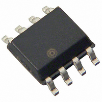
... Figure 3–21. Altera Serial Configuration Device 8-Pin SOIC Package Pin-Out Diagram Figure 3–22 shows the Altera serial configuration device 16-pin SOIC package and its pin-out diagram. Figure 3–22. Altera Serial Configuration Device 16-Pin SOIC Package Pin-Out Diagram Note to Figure 3–22: (1) These pins can be left floating or connected to V Table 3– ...
Page 34
... EPCS16 available in 8-pin and 16-pin small outline integrated circuit (SOIC) packages. EPCS64 and EPCS128 available in 16-pin small outline integrated circuit (SOIC) package. f For more information about Altera device packaging including mechanical drawing and specifications for this package, refer to the Sheet. Configuration Handbook (Complete Two-Volume Set) ...
Page 35
... Updated new document format. Updated Table 4–3, Table 4–6, Table 4–7, Table 4–28, and Table 4–29. Deleted Note 5 to Table 4–31. Added “Referenced Documents” section. Configuration Handbook (Complete Two-Volume Set) 3–35 Ordering Code (1) EPCS1SI8 EPCS1SI8N EPCS4SI8 EPCS4SI8N EPCS16SI16N EPCS16SI8N EPCS64SI16N EPCS128SI16N sections. ...
Page 36
... Updated DCLK pin information in Table 4–32. Updated Figure 4–19. Updated Table 4–30 and Table 4–32. Updated table 4-4 to include EPCS64 support for Cyclone devices. Updated tables. Minor text updates. Updated hot socketing AC specifications. Chapter Revision History © December 2009 Altera Corporation ...
Page 37
... July 2003 1.1 ■ May 2003 1.0 ■ © December 2009 Altera Corporation Changes Made Added Serial Configuration Device Memory Access section. Updated timing information in Tables 4–10 and 4–11 section. Updated timing information in Tables 4-16 and 4-17. Minor updates. Added document to the Cyclone Device Handbook. ...
Page 38
... Chapter 3: Serial Configuration Devices (EPCS1, EPCS4, EPCS16, EPCS64, and EPCS128) Data Sheet Configuration Handbook (Complete Two-Volume Set) Chapter Revision History © December 2009 Altera Corporation ...