EPCS4SI8 Altera, EPCS4SI8 Datasheet - Page 16
EPCS4SI8
Manufacturer Part Number
EPCS4SI8
Description
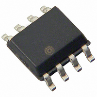
IC CONFIG DEVICE 4MBIT 8-SOIC
Manufacturer
Altera
Series
EPCSr
Datasheet
1.EPCS1SI8.pdf
(38 pages)
Specifications of EPCS4SI8
Programmable Type
In System Programmable
Memory Size
4Mb
Voltage - Supply
3 V ~ 3.6 V
Operating Temperature
-40°C ~ 85°C
Package / Case
8-SOIC (0.154", 3.90mm Width)
Lead Free Status / RoHS Status
Contains lead / RoHS non-compliant
Other names
544-1243-5
Available stocks
Company
Part Number
Manufacturer
Quantity
Price
Company:

Part Number:
EPCS4SI8
Manufacturer:
ST
Quantity:
6 251
Company:
Part Number:
EPCS4SI8
Manufacturer:
ALTERA44
Quantity:
66
Part Number:
EPCS4SI8
Manufacturer:
ALTERA/阿尔特拉
Quantity:
20 000
Company:
Part Number:
EPCS4SI8N
Manufacturer:
ALTERA
Quantity:
750
Part Number:
EPCS4SI8N
Manufacturer:
ALTERA/阿尔特拉
Quantity:
20 000


3–16
Configuration Handbook (Complete Two-Volume Set)
Write Disable Operation
The write disable operation code is b'0000 0100, with the MSB listed first. The
write disable operation resets the write enable latch bit, which is bit 1 in the status
register. To prevent the memory from being written unintentionally, the write enable
latch bit is automatically reset when implementing the write disable operation as well
as under the following conditions:
■
■
■
■
■
Figure 3–6
Figure 3–6. Write Disable Operation Timing Diagram
Read Status Operation
The read status operation code is b'0000 0101, with the MSB listed first. You can
use the read status operation to read the status register.
show the status bits in the status register of the serial configuration devices.
Figure 3–7. EPCS4, EPCS16, EPCS64, and EPCS128 Status Register Status Bits
Figure 3–8. EPCS1 Status Register Status Bits
Setting the write in progress bit to 1 indicates that the serial configuration device is
busy with a write or erase cycle. Resetting the write in progress bit to 0 means no
write or erase cycle is in progress.
Power up
Write bytes operation completion
Write status operation completion
Erase bulk operation completion
Erase sector operation completion
shows the timing diagram for the write disable operation.
Chapter 3: Serial Configuration Devices (EPCS1, EPCS4, EPCS16, EPCS64, and EPCS128) Data Sheet
DCLK
DATA
ASDI
nCS
Bit 7
Bit 7
High Impedance
0
1
BP2
Block Protect Bits [2..0]
2
Operation Code
BP1
BP1
Block Protect
3
Bits [1..0]
4
BP0
BP0
5
Write Enable
Write Enable
Latch Bit
Latch Bit
WEL
WEL
6
Serial Configuration Device Memory Access
Progress Bit
Progress Bit
7
Figure 3–7
Write In
Write In
WIP
Bit 0
WIP
Bit 0
© December 2009
and
Figure 3–8
Altera Corporation
Related parts for EPCS4SI8
Image
Part Number
Description
Manufacturer
Datasheet
Request
R


Part Number:
Description:
IC CONFIG DEVICE 1MBIT 8-DIP
Manufacturer:
Altera
Datasheet:

Part Number:
Description:
IC CONFIG DEVICE 1.6MBIT 20-PLCC
Manufacturer:
Altera
Datasheet:
Part Number:
Description:
IC CONFIG DEVICE 1.6MBIT 20-PLCC
Manufacturer:
Altera
Datasheet:

Part Number:
Description:
IC CONFIG DEVICE 1.6MBIT 32-TQFP
Manufacturer:
Altera
Datasheet:
Part Number:
Description:
IC CONFIG DEVICE 1.6MBIT 32-TQFP
Manufacturer:
Altera
Datasheet:
Part Number:
Description:
IC CONFIG DEVICE 1.6MBIT 20-PLCC
Manufacturer:
Altera
Datasheet:
Part Number:
Description:
IC CONFIG DEVICE 1.6MBIT 20-PLCC
Manufacturer:
Altera
Datasheet:

Part Number:
Description:
IC CONFIG DEVICE 8MBIT 100-PQFP
Manufacturer:
Altera
Datasheet:
Part Number:
Description:
IC CONFIG DEVICE 1.6MBIT 32-TQFP
Manufacturer:
Altera
Datasheet:
Part Number:
Description:
IC CONFIG DEVICE 1.6MBIT 32-TQFP
Manufacturer:
Altera
Datasheet:
Part Number:
Description:
IC CONFIG DEVICE 16MBIT 100-PQFP
Manufacturer:
Altera
Datasheet:
Part Number:
Description:
IC CONFIG DEVICE 16MBIT 100-PQFP
Manufacturer:
Altera
Datasheet:
Part Number:
Description:
IC CONFIG DEVICE 16MBIT 100-PQFP
Manufacturer:
Altera
Datasheet:

Part Number:
Description:
IC CONFIG DEVICE 16MBIT 88-UBGA
Manufacturer:
Altera
Datasheet: