EPCS4SI8 Altera, EPCS4SI8 Datasheet - Page 33
EPCS4SI8
Manufacturer Part Number
EPCS4SI8
Description
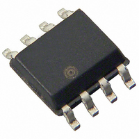
IC CONFIG DEVICE 4MBIT 8-SOIC
Manufacturer
Altera
Series
EPCSr
Datasheet
1.EPCS1SI8.pdf
(38 pages)
Specifications of EPCS4SI8
Programmable Type
In System Programmable
Memory Size
4Mb
Voltage - Supply
3 V ~ 3.6 V
Operating Temperature
-40°C ~ 85°C
Package / Case
8-SOIC (0.154", 3.90mm Width)
Lead Free Status / RoHS Status
Contains lead / RoHS non-compliant
Other names
544-1243-5
Available stocks
Company
Part Number
Manufacturer
Quantity
Price
Company:

Part Number:
EPCS4SI8
Manufacturer:
ST
Quantity:
6 251
Company:
Part Number:
EPCS4SI8
Manufacturer:
ALTERA44
Quantity:
66
Part Number:
EPCS4SI8
Manufacturer:
ALTERA/阿尔特拉
Quantity:
20 000
Company:
Part Number:
EPCS4SI8N
Manufacturer:
ALTERA
Quantity:
750
Part Number:
EPCS4SI8N
Manufacturer:
ALTERA/阿尔特拉
Quantity:
20 000


Chapter 3: Serial Configuration Devices (EPCS1, EPCS4, EPCS16, EPCS64, and EPCS128) Data Sheet
Pin Information
Pin Information
Table 3–23. Serial Configuration Device Pin Description (Part 1 of 2)
© December 2009
DATA
ASDI
Name
Pin
2
5
Pin Number
Package
in 8-Pin
SOIC
Altera Corporation
As shown in
16-pin device. The control pins on the serial configuration device are: serial data
output (DATA), active serial data input (ASDI), serial clock (DCLK), and chip select
(nCS).
Figure 3–21
pin-out diagram.
Figure 3–21. Altera Serial Configuration Device 8-Pin SOIC Package Pin-Out Diagram
Figure 3–22
pin-out diagram.
Figure 3–22. Altera Serial Configuration Device 16-Pin SOIC Package Pin-Out Diagram
Note to
(1) These pins can be left floating or connected to V
8
15
Pin Number
in 16-Pin
Package
Figure
SOIC
Table 3–23
3–22:
shows the Altera serial configuration device 8-pin SOIC package and its
shows the Altera serial configuration device 16-pin SOIC package and its
Figure 3–21
Output
Input
Pin Type
lists the serial configuration device's pin descriptions.
and
The DATA output signal transfers data serially out of the serial
configuration device to the FPGA during read/configuration operation.
During read/configuration operations, the serial configuration device
is enabled by pulling nCS low. The DATA signal transitions on the
falling edge of DCLK.
The AS data input signal is used to transfer data serially into the serial
configuration device. It receives the data that should be programmed
into the serial configuration device. Data is latched on the rising edge
of DCLK.
Figure
DATA
DATA
GND
nCS
V
N.C.
N.C.
N.C.
N.C.
nCS
V
V
CC
CC
CC
3–22, the serial configuration device is an 8-pin or
CC
EPCS1, EPCS4,
or EPCS128
or GND, whichever is more convenient on the board.
or EPCS16
1
2
3
4
EPCS64,
2
3
4
5
6
7
8
EPCS16,
1
(1)
(1)
(1)
(1)
14
13
12
11
10
9
16
15
8
7
6
5
(1)
(1)
(1)
(1)
Configuration Handbook (Complete Two-Volume Set)
V
V
DCLK
ASDI
DCLK
ASDI
N.C.
N.C.
N.C.
N.C.
GND
V
CC
CC
CC
Description
3–33
Related parts for EPCS4SI8
Image
Part Number
Description
Manufacturer
Datasheet
Request
R


Part Number:
Description:
IC CONFIG DEVICE 1MBIT 8-DIP
Manufacturer:
Altera
Datasheet:

Part Number:
Description:
IC CONFIG DEVICE 1.6MBIT 20-PLCC
Manufacturer:
Altera
Datasheet:
Part Number:
Description:
IC CONFIG DEVICE 1.6MBIT 20-PLCC
Manufacturer:
Altera
Datasheet:

Part Number:
Description:
IC CONFIG DEVICE 1.6MBIT 32-TQFP
Manufacturer:
Altera
Datasheet:
Part Number:
Description:
IC CONFIG DEVICE 1.6MBIT 32-TQFP
Manufacturer:
Altera
Datasheet:
Part Number:
Description:
IC CONFIG DEVICE 1.6MBIT 20-PLCC
Manufacturer:
Altera
Datasheet:
Part Number:
Description:
IC CONFIG DEVICE 1.6MBIT 20-PLCC
Manufacturer:
Altera
Datasheet:

Part Number:
Description:
IC CONFIG DEVICE 8MBIT 100-PQFP
Manufacturer:
Altera
Datasheet:
Part Number:
Description:
IC CONFIG DEVICE 1.6MBIT 32-TQFP
Manufacturer:
Altera
Datasheet:
Part Number:
Description:
IC CONFIG DEVICE 1.6MBIT 32-TQFP
Manufacturer:
Altera
Datasheet:
Part Number:
Description:
IC CONFIG DEVICE 16MBIT 100-PQFP
Manufacturer:
Altera
Datasheet:
Part Number:
Description:
IC CONFIG DEVICE 16MBIT 100-PQFP
Manufacturer:
Altera
Datasheet:
Part Number:
Description:
IC CONFIG DEVICE 16MBIT 100-PQFP
Manufacturer:
Altera
Datasheet:

Part Number:
Description:
IC CONFIG DEVICE 16MBIT 88-UBGA
Manufacturer:
Altera
Datasheet: