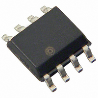
EPCS4SI8 Altera, EPCS4SI8 Datasheet - Page 5

EPCS4SI8
Manufacturer Part Number
EPCS4SI8
Description
IC CONFIG DEVICE 4MBIT 8-SOIC
Manufacturer
Altera
Series
EPCSr
Datasheet
1.EPCS1SI8.pdf
(38 pages)
Specifications of EPCS4SI8
Programmable Type
In System Programmable
Memory Size
4Mb
Voltage - Supply
3 V ~ 3.6 V
Operating Temperature
-40°C ~ 85°C
Package / Case
8-SOIC (0.154", 3.90mm Width)
Lead Free Status / RoHS Status
Contains lead / RoHS non-compliant
Other names
544-1243-5
Available stocks
Company
Part Number
Manufacturer
Quantity
Price
Company:
Part Number:
EPCS4SI8
Manufacturer:
ST
Quantity:
6 251
Company:
Part Number:
EPCS4SI8
Manufacturer:
ALTERA44
Quantity:
66
Part Number:
EPCS4SI8
Manufacturer:
ALTERA/阿尔特拉
Quantity:
20 000
Company:
Part Number:
EPCS4SI8N
Manufacturer:
ALTERA
Quantity:
750
Part Number:
EPCS4SI8N
Manufacturer:
ALTERA/阿尔特拉
Quantity:
20 000
Chapter 3: Serial Configuration Devices (EPCS1, EPCS4, EPCS16, EPCS64, and EPCS128) Data Sheet
Active Serial FPGA Configuration
Figure 3–3. Altera FPGA Configuration in AS Mode (Serial Configuration Device Programmed by APU or Third-Party
Programmer)
Notes to
(1) For the V
(2) Serial configuration devices cannot be cascaded.
(3) Connect the FPGA MSEL[] input pins to select the AS configuration mode. For details, refer to the respective FPGA family chapter in the
(4) For more information about configuration pin I/O requirements in an AS scheme for an Altera FPGA, refer to the respective FPGA family handbook
© December 2009
Configuration
Configuration chapter..
Figure
CC
value, refer to the respective FPGA family handbook Configuration chapter.
f
(Note
3–3:
1
Handbook.
Altera Corporation
1),
The FPGA acts as the configuration master in the configuration flow and provides the
clock to the serial configuration device. The FPGA enables the serial configuration
device by pulling the nCS signal low via the nCSO signal (refer to
Figure
configuration device via the ASDO signal. The serial configuration device responds to
the instructions by sending the configuration data to the FPGA’s DATA0 pin on the
falling edge of DCLK. The data is latched into the FPGA on the next DCLK signal’s
falling edge.
Before the FPGA enters configuration mode, ensure that V
is not, you must hold nCONFIG low until all power rails of EPCS are ready.
The FPGA controls the nSTATUS and CONF_DONE pins during configuration in AS
mode. If the CONF_DONE signal does not go high at the end of configuration or if the
signal goes high too early, the FPGA will pulse its nSTATUS pin low to start
reconfiguration. Upon successful configuration, the FPGA releases the CONF_DONE
pin, allowing the external 10-k resistor to pull this signal high. Initialization begins
after the CONF_DONE goes high. After initialization, the FPGA enters user mode.
For more information about configuring the FPGAs in AS mode or other
configuration modes, refer to the Configuration chapter in the appropriate device
handbook.
(4)
3–3). Subsequently, the FPGA sends the instructions and addresses to the serial
Configuration
Device (2)
Serial
DATA
DCLK
ASDI
nCS
10 k
V
CC
(1)
10 k
V
CC
(1) V
CC
10 k
(1)
CONF_DONE
nSTATUS
nCONFIG
nCE
DATA0
DCLK
nCSO
ASDO
Altera FPGA
Configuration Handbook (Complete Two-Volume Set)
MSEL[]
nCEO
N.C.
(3)
CC
of the EPCS is ready. If it
Figure 3–2
and
3–5


